
Page 281 - Fundamentals of Light Microscopy and Electronic Imaging
P. 281
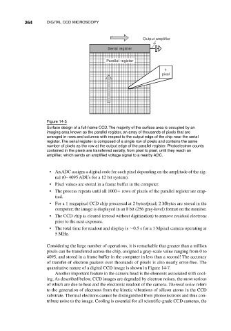
264      DIGITAL CCD MICROSCOPY


                                                                          Output amplifier

                                                           Serial register

                                                          Parallel register
                                                                                    1
                                                                                  pixel


                                Figure 14-5
                                Surface design of a full-frame CCD. The majority of the surface area is occupied by an
                                imaging area known as the parallel register, an array of thousands of pixels that are
                                arranged in rows and columns with respect to the output edge of the chip near the serial
                                register. The serial register is composed of a single row of pixels and contains the same
                                number of pixels as the row at the output edge of the parallel register. Photoelectron counts
                                contained in the pixels are transferred serially, from pixel to pixel, until they reach an
                                amplifier, which sends an amplified voltage signal to a nearby ADC.


                                 • An ADC assigns a digital code for each pixel depending on the amplitude of the sig-
                                    nal (0–4095 ADUs for a 12 bit system).
                                 • Pixel values are stored in a frame buffer in the computer.
                                 • The process repeats until all 1000  rows of pixels of the parallel register are emp-
                                    tied.
                                 • For a 1 megapixel CCD chip processed at 2 bytes/pixel, 2 Mbytes are stored in the
                                    computer; the image is displayed in an 8 bit (256 gray-level) format on the monitor.
                                 • The CCD chip is cleared (reread without digitization) to remove residual electrons
                                    prior to the next exposure.
                                 • The total time for readout and display is  0.5 s for a 1 Mpixel camera operating at
                                    5 MHz.

                                Considering the large number of operations, it is remarkable that greater than a million
                                pixels can be transferred across the chip, assigned a gray-scale value ranging from 0 to
                                4095, and stored in a frame buffer in the computer in less than a second! The accuracy
                                of transfer of electron packets over thousands of pixels is also nearly error-free. The
                                quantitative nature of a digital CCD image is shown in Figure 14-7.
                                    Another important feature in the camera head is the elements associated with cool-
                                ing. As described below, CCD images are degraded by electron noises, the most serious
                                of which are due to heat and the electronic readout of the camera. Thermal noise refers
                                to the generation of electrons from the kinetic vibrations of silicon atoms in the CCD
                                substrate. Thermal electrons cannot be distinguished from photoelectrons and thus con-
                                tribute noise to the image. Cooling is essential for all scientific-grade CCD cameras, the