
Page 278 - Fundamentals of Light Microscopy and Electronic Imaging
P. 278
THE CHARGE-COUPLED DEVICE (CCD IMAGER) 261
CCD
camera
Camera control
unit
Computer
Microscope
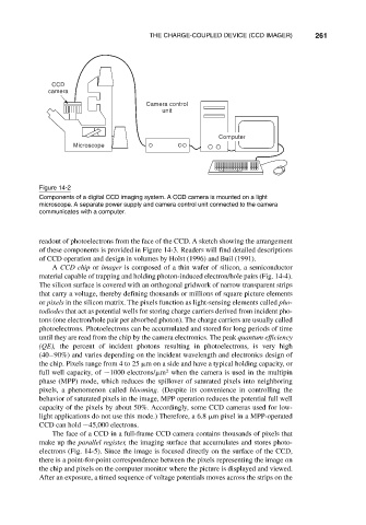
Figure 14-2
Components of a digital CCD imaging system. A CCD camera is mounted on a light
microscope. A separate power supply and camera control unit connected to the camera
communicates with a computer.
readout of photoelectrons from the face of the CCD. A sketch showing the arrangement
of these components is provided in Figure 14-3. Readers will find detailed descriptions
of CCD operation and design in volumes by Holst (1996) and Buil (1991).
A CCD chip or imager is composed of a thin wafer of silicon, a semiconductor
material capable of trapping and holding photon-induced electron/hole pairs (Fig. 14-4).
The silicon surface is covered with an orthogonal gridwork of narrow transparent strips
that carry a voltage, thereby defining thousands or millions of square picture elements
or pixels in the silicon matrix. The pixels function as light-sensing elements called pho-
todiodes that act as potential wells for storing charge carriers derived from incident pho-
tons (one electron/hole pair per absorbed photon). The charge carriers are usually called
photoelectrons. Photoelectrons can be accumulated and stored for long periods of time
until they are read from the chip by the camera electronics. The peak quantum efficiency
(QE), the percent of incident photons resulting in photoelectrons, is very high
(40–90%) and varies depending on the incident wavelength and electronics design of
the chip. Pixels range from 4 to 25 m on a side and have a typical holding capacity, or
2
full well capacity, of 1000 electrons/ m when the camera is used in the multipin
phase (MPP) mode, which reduces the spillover of saturated pixels into neighboring
pixels, a phenomenon called blooming. (Despite its convenience in controlling the
behavior of saturated pixels in the image, MPP operation reduces the potential full well
capacity of the pixels by about 50%. Accordingly, some CCD cameras used for low-
light applications do not use this mode.) Therefore, a 6.8 m pixel in a MPP-operated
CCD can hold 45,000 electrons.
The face of a CCD in a full-frame CCD camera contains thousands of pixels that
make up the parallel register, the imaging surface that accumulates and stores photo-
electrons (Fig. 14-5). Since the image is focused directly on the surface of the CCD,
there is a point-for-point correspondence between the pixels representing the image on
the chip and pixels on the computer monitor where the picture is displayed and viewed.
After an exposure, a timed sequence of voltage potentials moves across the strips on the