
Page 280 - Fundamentals of Light Microscopy and Electronic Imaging
P. 280
THE CHARGE-COUPLED DEVICE (CCD IMAGER) 263
Red
Blue photon
photon
X ray
High-
energy
particle
Thermal
energy
zap
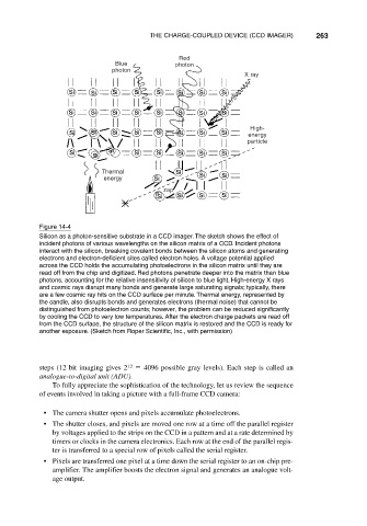
Figure 14-4
Silicon as a photon-sensitive substrate in a CCD imager. The sketch shows the effect of
incident photons of various wavelengths on the silicon matrix of a CCD. Incident photons
interact with the silicon, breaking covalent bonds between the silicon atoms and generating
electrons and electron-deficient sites called electron holes. A voltage potential applied
across the CCD holds the accumulating photoelectrons in the silicon matrix until they are
read off from the chip and digitized. Red photons penetrate deeper into the matrix than blue
photons, accounting for the relative insensitivity of silicon to blue light. High-energy X rays
and cosmic rays disrupt many bonds and generate large saturating signals; typically, there
are a few cosmic ray hits on the CCD surface per minute. Thermal energy, represented by
the candle, also disrupts bonds and generates electrons (thermal noise) that cannot be
distinguished from photoelectron counts; however, the problem can be reduced significantly
by cooling the CCD to very low temperatures. After the electron charge packets are read off
from the CCD surface, the structure of the silicon matrix is restored and the CCD is ready for
another exposure. (Sketch from Roper Scientific, Inc., with permission)
steps (12 bit imaging gives 2 12 4096 possible gray levels). Each step is called an
analogue-to-digital unit (ADU).
To fully appreciate the sophistication of the technology, let us review the sequence
of events involved in taking a picture with a full-frame CCD camera:
• The camera shutter opens and pixels accumulate photoelectrons.
• The shutter closes, and pixels are moved one row at a time off the parallel register
by voltages applied to the strips on the CCD in a pattern and at a rate determined by
timers or clocks in the camera electronics. Each row at the end of the parallel regis-
ter is transferred to a special row of pixels called the serial register.
• Pixels are transferred one pixel at a time down the serial register to an on-chip pre-
amplifier. The amplifier boosts the electron signal and generates an analogue volt-
age output.