
Page 279 - Handbook of Lasers
P. 279
Section 1.5
SEMICONDUCTOR LASERS
1.5.1 Introduction
Laser action in semiconductor diode lasers, in contrast to other solid state lasers, is
associated with radiative recombination of electrons and holes at the junction of a n-type
material (excess electrons) and a p-type material (excess holes). Excess charge is injected into
the active region via an external electric field applied across a simple p-n junction
(homojunction) or in a heterostructure consisting of several layers of semiconductor materials
that have different band gap energies but are lattice matched. The ability to grow special
structures one atomic layer at a time by liquid phase epitaxy (LPE), molecular bean epitaxy
(MBE), and metal-organic chemical vapor deposition (MOCVD) has led to an explosive
growth of activity and numerous new laser structures and configurations.
When the dimensions of the semiconductor material become <100 nm, quantum effects
enter that modify the band gap. Quantum wells result from confinement in one dimension,
quantum wires from confinement in two dimensions, and quantum dots or boxes from
confinement in three dimensions. The wavelength of quantum well lasers can be changed by
varying the quantum well thickness or the composition of the active material. By using
materials of different lattice constants, thereby effectively straining the materials, one can
further engineer the band gap.
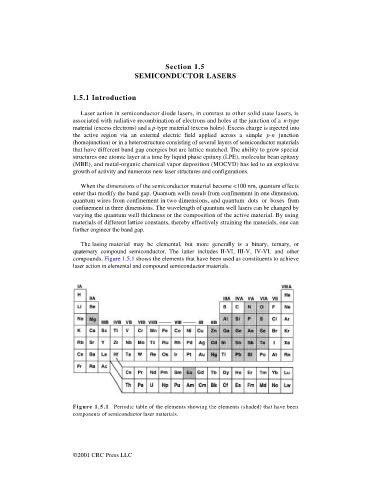
The lasing material may be elemental, but more generally is a binary, ternary, or
quaternary compound semiconductor. The latter includes II-VI, III-V, IV-VI, and other
compounds. Figure 1.5.1 shows the elements that have been used as constituents to achieve
laser action in elemental and compound semiconductor materials.
Figure 1.5.1 Periodic table of the elements showing the elements (shaded) that have been
components of semiconductor laser materials.
©2001 CRC Press LLC