
Page 547 - Instrumentation Reference Book 3E
P. 547
Detectors 529
the faces. If the resistivity of this material is thermal processes. By reducing the temperature
2000 61 cm, with ohmic contacts on each side, then of the detector by liquid nitrogen to about IT E;
the skice would behave like a resistor of 2000, most of this background is removed, but in prac-
and if 100%’ is applied across such a resistor then tical detectors the effect of surface contaminants
Ol1m’:s Law states that a current of 0.5 A would on those surfaces not forming the diode can be
pass. If radiation now falls on the silicon slice, a acute. Various methods of avoiding these pro-
minute extra current will be produced, but this blems, such as the use of guard rings, have
would! be so small compared with the standing reduced much of this problem. However, the
0.5 A curreiit that it would be undetectable. This effects of very small amounts of oxygen, etc,; can
is different from the gas-ionization chamber, have devastating results on a detector, 2nd most
\&ere the standing current is extremely small. are enclosed in a h~gh-~7acuu~ chaniber.
The so~~~tio1~ to this problem is provided by semi- By doping a ~erman~u~ or silicon crystal with
(an
conductor junctions. The operation of junctions l~tl~~um ~nterstiti~ donorj, which is carried
depends on the fact that a mass action law com- out at moderate t~rnpe~~~ures using an electric
pels the product of electron and hole concentra- field across the crystal, the acceptors can be
compensate^ in p-type silicon
tions to be constant for a given semiconductor at almost eoii~plete13~
a fixed ~empe~ature. Therefore. heavy doping and germanium, This allows the preparation of
with a donor such as phospho~~Is not only relatively large detectors suitable for high-energy
increases the free electron concentration but also charged particle spectroscopy. By this nieaiis
depresses the hole Concentration to satisfy the coaxial detectors with volumes up to about
relation that the product IT~LIS~ have a valse 100 cm3 have been made, and these have revolu-
dependent only on the semiconductor. For exam- tionized gamma-ray spectroscopy, as they can
ple, silicon at room temperature has the relation separate energy lines in a spectrum which earlier
n x IJ z 10”. where YL is the number of holes and NaI (Tl) scintillation spectrometers could not
p is t:he number of electrons. Hence in a region resolve.
where the number of donors is doped to a con- New work on purifying germanium and silicon
centration of 1Q18 the number of holes will be has resulted in the manufacture of detectors of
reduced to about 10‘. McKay, of Bell Telephone super-pure quality such that lithium drifting is
Laboratories, first demonstrated in 1949 that ifa not required. Detectors made from such material
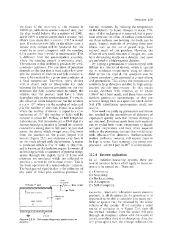
reverse-biased pa junction is formed on the semi- can be cycled from room temperature to liquid-
conductor a strong electric field may be provided nitrogen temperature and back when required
across the device which sweeps away free holes without the permanent damage that would QCCW
from the junction on the y-side (doped with with lithium-drifted detectors. SurFace-contam-
boron) (Figure 22.5) and electrons away from it ination problems, however, still require them to
on ?he n-side (doped with phosphorus). A region be kept in IJLICUO. Such materia! is the purest ever
is produced which is free of holes or electrons, produced-about 1 part in 10’’ of contaminants.
and is kno-cvi: as the depletion region. However. if
an ionizing particle or quantum of gamma energy
passes through the region. pairs of holes and 22.2.4 Detector applications
electrons are produced which are collected to Iii a11 radiation-measuring systems there are
produce a current in the external circuit. This is several common factors which apply to measure-
the basic operation of a semiconductor detector. ments to be carried out. These are:
The ttackground signal is due to the collection of
any pairs of holes plus electrons produced by (1) Geometry;
(2) Scattering:
(3) Bac~scait~rin~:
toad
resistance (4) Absorp~ion;
(5) Self-absorp~ion.
~
~
~
Electron motion ~ e Since any radioacxive source emits ~its ~ ~ ~ !
products in all directions (in 4?i geometry) it Is
Depletion
region important 10 be able to calculate how many par-
Hole motion ticles or quanta may be collected by the active
volume of the counter. If we consider a point
source of radiation as in Figure 22.6, then all
the emitted radiation from the source will pass
through an imaginary sphere with the source at
Figure 22.5 Schematic diagram ofsemiconductor center, providing there is no absorption. Also, for
derector any given sphere size. the average radiation flux