
Page 213 - Introduction to Information Optics
P. 213
198 3. Communication with Optics
Fiber optic link under test
Stimulus Receiver
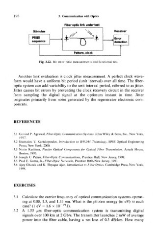
Fig. 3.22. Bit error ratio measurements and functional test.
Another link evaluation is clock jitter measurement. A perfect clock wave-
form would have a uniform bit period (unit interval) over all time. The fiber-
optic system can add variability to the unit interval period, referred to as jitter.
Jitter causes bit errors by preventing the clock recovery circuit in the receiver
from sampling the digital signal at the optimum instant in time. Jitter
originates primarily from noise generated by the regenerator electronic com-
ponents.
REFERENCES
3.1 Govind P. Agrawal, Fiber-Optic Communication Systems, John Wiley & Sons, Inc., New York,
1997.
3.2 Stamatios V. Kartalopoulos, Introduction to DWDM Technology, SPIE Optical Engineering
Press, New York, 2000.
3.3 Norio Kashima, Passive Optical Components for Optical Fiber Transmission, Artech House,
Boston, 1995.
3.4 Joseph C. Palais, Fiber-Optic Communications, Prentice Hall, New Jersey, 1998.
3.5 Paul E, Green, Jr., Fiber-Optic Networks, Prentice Hall, New Jersey, 1993.
3.6 Ajoy Ghatak and K. Thyagar Ajan, Introduction to Fiber Optics, Cambridge Press, New York,
1998.
EXERCISES
3.1 Calculate the carrier frequency of optical communication systems operat-
ing at 0.88, 1.3, and 1.55 /mi. What is the photon energy (in eV) in each
19
case?(l eV = 1.6 x 1(T J).
3.2 A 1.55 /j,m fiber-optic communication system is transmitting digital
signals over 100 km at 2 Gb/s. The transmitter launches 2 mW of average
power into the fiber cable, having a net loss of 0.3 dB/km. How many