
Page 248 - Introduction to Information Optics
P. 248
4.3. Fast Electro-optic Switches: Modulators 253
bandgap material. Because of thin wells, the behavior of electrons and holes in
these two-dimensional (2D) potentials alters their density-of-states functions in
such a way that the absorption edge is sharpened. In addition, the motion of
electrons and holes is constrained by their confinement, leading to discrete
energy levels in the wells. Because of the 2D nature of the electron -hole gas in
quantum wells, exciton binding energy is increased with respect to the bulk
semiconductor so as to make excitons observable at room temperature in the
absorption spectrum of MQW.
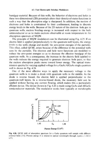
The principle of MQW modulators can be illustrated using Fig. 4.25. If an
electric field is applied perpendicularly to the quantum-well layers, the energy
levels in the wells change and modify the zero-point energies of the particles.
This effect, called QCSE, arises because of the difference in the potential wells
seen by the particles. The electron and hole wave functions are modified to
reduce the zero-point energies so as to decrease the effective bandgap of the
quantum wells. As a consequence, the increase in the electric field applied to
the wells reduces the energy required to generate electron hole pairs, so that
the exciton absorption peaks move toward lower energy. The optical trans-
mission spectra for varying applied voltage for a GaAs/AlGaAs single quantum
well is shown in Fig. 4.26.
One of the most effective ways to apply the necessary voltage to the
quantum wells is to make a diode with quantum wells in the middle. As the
diode is reverse biased, the electric field is applied perpendicular to the
quantum-well layers. In a reverse-biased diode, the necessary field can be
applied without having any current flowing, which makes this a particularly
efficient device. The device shown in Fig. 4.26 is made using GaAs and AlGaAs
semiconductor materials. The modulator works best typically at wavelengths
10 4
V = OV
6V
ti
I
I
1.43 Eo 1.48
Photon Energy E (eV)
Fig. 4.26. QCSE shift of absorption spectrum for a GaAs quantum well sample with different
external fields [31]. Photon energy E is related to optical wavelength through },(nm) = 1.242/E
(eV).