
Page 250 - Introduction to Information Optics
P. 250
4.3. Fast Electro-optic Switches: Modulators
MQW
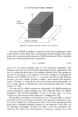
Fig. 4.27. Waveguide multiple quantum-well modulator.
The speed of MQW modulators is limited by the resistor-capacitance limits
of the external circuits. Both time- and frequency-domain measures have been
performed to characterize the response of MQW modulators. With a simplified
model, the 3-dB bandwidth bias is expressed as
A/ = l/(2nRC), (4.45)
where R is the source resistance and C is the modulator capacitance. The
frequency response can be increased by decreasing the device capacitance. One
way is to reduce the device area to the smallest practical value. The capacitance
can also be decreased at the expense of the drive voltage by increasing the
thickness of the MQW layer in the p-i-n junction. However, as this thickness
increases, the drive voltage required to obtain a given electric field increases
linearly. Therefore, a trade-off must be made between device bandwidth and
drive voltage. Speeds of 40 GHz have been demonstrated with drive voltage
around 2 V [34].
As in the case for LiNbO 3 modulators, bandwidth of EA MQW modulators
can be increased by using traveling wave (TW) electrodes (Fig. 4.21). MQW
modulators with 50 GHz bandwidth, 15 dB on-off ratio, and <2 V drive
voltage have been demonstrated using such a configuration [35].
Several effects contribute to device insertion loss. The main effect is residual
absorption by the semiconductor material in the maximum transmission state
due to loss of band tails of the quantum wells or free carrier absorption in the
doped layers. Residual absorption depends on the materials of the QWs and
the operating wavelength. Another loss effect is the one associated with
reflection off its facets. For semiconductors of interest, a typical value of the