
Page 260 - Introduction to Information Optics
P. 260
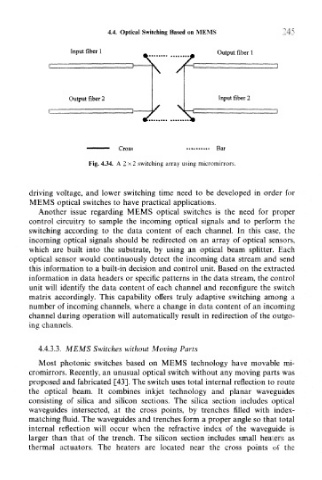
4.4. Optical Switching Based on MEMS         245

                  Input fiber 1                        Output fiber i
             1                    1   2        £_,
                                       \ X


                  Output fiber 2                       Input fiber 2
                                       X     N s                      ,

             '                    ^


                              Cross            ••    • Bar
                       Fig. 4.34. A 2 x 2 switching array using micromirrors.


        driving voltage, and lower switching time need to be developed in order for
        MEMS optical switches to have practical applications.
          Another issue regarding MEMS optical switches is the need for proper
        control circuitry to sample the incoming optical signals and to perform the
        switching according to the data content of each channel. In this case, the
        incoming optical signals should be redirected on an array of optical sensors,
        which are built into the substrate, by using an optical beam splitter. Each
        optical sensor would continuously detect the incoming data stream and send
        this information to a built-in decision and control unit. Based on the extracted
        information in data headers or specific patterns in the data stream, the control
        unit will identify the data content of each channel and reconfigure the switch
        matrix accordingly. This capability offers truly adaptive switching among a
        number of incoming channels, where a change in data content of an incoming
        channel during operation will automatically result in redirection of the outgo-
        ing channels.


          4.4.3.3. MEMS Switches without Moving Parts
          Most photonic switches based on MEMS technology have movable mi-
        cromirrors. Recently, an unusual optical switch without any moving parts was
        proposed and fabricated [43]. The switch uses total internal reflection to route
        the optical beam. It combines inkjet technology and planar waveguides
        consisting of silica and silicon sections. The silica section includes optical
        waveguides intersected, at the cross points, by trenches filled with index-
        matching fluid. The waveguides and trenches form a proper angle so that total
        internal reflection will occur when the refractive index of the waveguide is
        larger than that of the trench. The silicon section includes small heaters as
        thermal actuators. The heaters are located near the cross points of the