
Page 267 - Introduction to Information Optics
P. 267
252 4. Switching with Optics
\
Waveguide
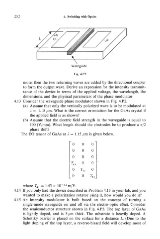
Fig. 4.P2.
more; then the two returning waves are added by the directional coupler
to form the output wave. Derive an expression for the intensity transmit-
tance of the device in terms of the applied voltage, the wavelength, the
dimensions, and the physical parameters of the phase modulator.
4.13 Consider the waveguide phase modulator shown in Fig. 4.P2.
(a) Assume that only the vertically polarized wave is to be modulated at
A = 1.15 /im. What is the correct orientation for the GaAs crystal if
the applied field is as shown?
(b) Assume that the electric field strength in the waveguide is equal to
100 (V/mm). What length should the electrodes be to produce a n/2
phase shift?
The EO tensor of GaAs at / = 1.15 /mi is given below.
~ 0 0 0 "
0 0 0
0 0 0
0 0
T 4l
0 T 41 0
0 0
T
41_
12
where T 41 = 1.43 x 10~ m/V.
4.14 If you only had the device described in Problem 4.13 in your lab, and you
wanted to make a polarization rotator using it, how would you do it?
4.15 An intensity modulator is built based on the concept of turning a
single-mode waveguide on and off via the electro-optic effect. Consider
the semiconductor structure shown in Fig. 4.P3. The top layer of GaAs
is lightly doped, and is 5 /mi thick. The substrate is heavily doped. A
Schottky barrier is placed on the surface for a distance L. (Due to the
light doping of the top layer, a reverse-biased field will develop most of