
Page 331 - Sami Franssila Introduction to Microfabrication
P. 331
310 Introduction to Microfabrication
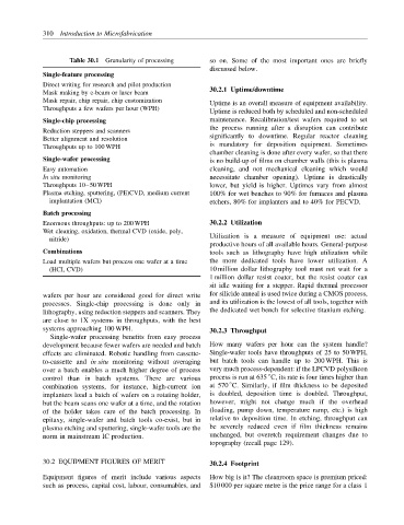
Table 30.1 Granularity of processing so on. Some of the most important ones are briefly
discussed below.
Single-feature processing
Direct writing for research and pilot production
Mask making by e-beam or laser beam 30.2.1 Uptime/downtime
Mask repair, chip repair, chip customization Uptime is an overall measure of equipment availability.
Throughputs a few wafers per hour (WPH)
Uptime is reduced both by scheduled and non-scheduled
Single-chip processing maintenance. Recalibration/test wafers required to set
the process running after a disruption can contribute
Reduction steppers and scanners
Better alignment and resolution significantly to downtime. Regular reactor cleaning
Throughputs up to 100 WPH is mandatory for deposition equipment. Sometimes
chamber cleaning is done after every wafer, so that there
Single-wafer processing is no build-up of films on chamber walls (this is plasma
Easy automation cleaning, and not mechanical cleaning which would
In situ monitoring necessitate chamber opening). Uptime is drastically
Throughputs 10–50 WPH lower, but yield is higher. Uptimes vary from almost
Plasma etching, sputtering, (PE)CVD, medium current 100% for wet benches to 90% for furnaces and plasma
implantation (MCI) etchers, 80% for implanters and to 40% for PECVD.
Batch processing
Enormous throughputs: up to 200 WPH 30.2.2 Utilization
Wet cleaning, oxidation, thermal CVD (oxide, poly,
nitride) Utilization is a measure of equipment use: actual
productive hours of all available hours. General-purpose
Combinations tools such as lithography have high utilization while
Load multiple wafers but process one wafer at a time the more dedicated tools have lower utilization. A
(HCI, CVD) 10 million dollar lithography tool must not wait for a
1 million dollar resist coater, but the resist coater can
sit idle waiting for a stepper. Rapid thermal processor
wafers per hour are considered good for direct write for silicide anneal is used twice during a CMOS process,
processes. Single-chip processing is done only in and its utilization is the lowest of all tools, together with
lithography, using reduction steppers and scanners. They the dedicated wet bench for selective titanium etching.
are close to 1X systems in throughputs, with the best
systems approaching 100 WPH. 30.2.3 Throughput
Single-wafer processing benefits from easy process
development because fewer wafers are needed and batch How many wafers per hour can the system handle?
effects are eliminated. Robotic handling from cassette- Single-wafer tools have throughputs of 25 to 50 WPH,
to-cassette and in situ monitoring without averaging but batch tools can handle up to 200 WPH. This is
over a batch enables a much higher degree of process very much process-dependent: if the LPCVD polysilicon
◦
control than in batch systems. There are various process is run at 635 C, its rate is four times higher than
◦
combination systems, for instance, high-current ion at 570 C. Similarly, if film thickness to be deposited
implanters load a batch of wafers on a rotating holder, is doubled, deposition time is doubled. Throughput,
but the beam scans one wafer at a time, and the rotation however, might not change much if the overhead
of the holder takes care of the batch processing. In (loading, pump down, temperature ramp, etc.) is high
epitaxy, single-wafer and batch tools co-exist, but in relative to deposition time. In etching, throughput can
plasma etching and sputtering, single-wafer tools are the be severely reduced even if film thickness remains
norm in mainstream IC production. unchanged, but overetch requirement changes due to
topography (recall page 129).
30.2 EQUIPMENT FIGURES OF MERIT 30.2.4 Footprint
Equipment figures of merit include various aspects How big is it? The cleanroom space is premium priced:
such as process, capital cost, labour, consumables, and $10 000 per square metre is the price range for a class 1