
Page 73 - MEMS Mechanical Sensors
P. 73
62 Mechanical Sensor Packaging
• Reduced package size;
• High-speed electrical performance due to the shortened path length;
• Greater flexibility of contact pad location;
• Mechanically rugged;
• Lowest cost interconnection method for high-volume production.
The disadvantages are similar to those associated with the TAB interconnects in
that the package or substrate must be custom made for different die designs. Also,
testing the quality of interconnects, repairing defects, and the relative complexity of
the assembly process are drawbacks as well.
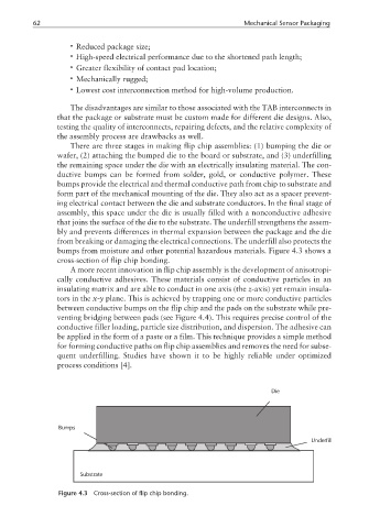
There are three stages in making flip chip assemblies: (1) bumping the die or
wafer, (2) attaching the bumped die to the board or substrate, and (3) underfilling
the remaining space under the die with an electrically insulating material. The con-
ductive bumps can be formed from solder, gold, or conductive polymer. These
bumps provide the electrical and thermal conductive path from chip to substrate and
form part of the mechanical mounting of the die. They also act as a spacer prevent-
ing electrical contact between the die and substrate conductors. In the final stage of
assembly, this space under the die is usually filled with a nonconductive adhesive
that joins the surface of the die to the substrate. The underfill strengthens the assem-
bly and prevents differences in thermal expansion between the package and the die
from breaking or damaging the electrical connections. The underfill also protects the
bumps from moisture and other potential hazardous materials. Figure 4.3 shows a
cross-section of flip chip bonding.
A more recent innovation in flip chip assembly is the development of anisotropi-
cally conductive adhesives. These materials consist of conductive particles in an
insulating matrix and are able to conduct in one axis (the z-axis) yet remain insula-
tors in the x-y plane. This is achieved by trapping one or more conductive particles
between conductive bumps on the flip chip and the pads on the substrate while pre-
venting bridging between pads (see Figure 4.4). This requires precise control of the
conductive filler loading, particle size distribution, and dispersion. The adhesive can
be applied in the form of a paste or a film. This technique provides a simple method
for forming conductive paths on flip chip assemblies and removes the need for subse-
quent underfilling. Studies have shown it to be highly reliable under optimized
process conditions [4].
Die
Bumps
Underfill
Substrate
Figure 4.3 Cross-section of flip chip bonding.