
Page 74 - MEMS Mechanical Sensors
P. 74
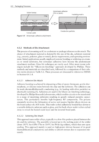
4.3 Packaging Processes                                                        63

                                                       Anisotropic adhesive
                            Solder bumps               (film or paste)
                                                                          Insulating matrix
                                              Chip


                                         Substrate
                                                               Conductive particles
                            Contact pads
                  Figure 4.4  Anisotropic adhesive attachment.


                  4.3.2  Methods of Die Attachment
                  The process of mounting an IC to a substrate or package is known as die attach. The
                  choice of attachment material is dictated by the size of the die, substrate material
                  (e.g., ceramic, polymer, glass or metal), device requirements, and operating environ-
                  ment. Initial applications usually employed eutectic bonding or soldering on ceram-
                  ics or metal substrates, but nowadays adhesives have become the predominant
                  attachment medium. Glass frit techniques are rarely used. Other more recent tech-
                  niques include the “Silicon-on-Anything” approach developed by Phillips. These
                  methods and materials are described next, followed by a comparison of their rela-
                  tive merits shown in Table 4.2. These processes are discussed in relation to MEMS
                  in Section 4.4.1.4.


                  4.3.2.1  Adhesive Die Attach
                  Adhesive bonding is achieved by depositing a film of epoxy thermoset, acrylic ther-
                  moplastic, or silicone resins between the chip and the substrate. The adhesives can
                  be made electrically/thermally conducting (e.g., by loading with silver particles) or
                  electrically isolating [5]. Adhesives are used in the Silicon-on-Anything technology,
                  developed by Philips Research Laboratories, which enables circuits to be transferred
                  to a range of insulating substrates resulting in greatly reduced parasitic capaci-
                  tances. This particularly benefits high-frequency RF components. The process
                  essentially involves the fabrication of active and passive bipolar silicon devices on
                  the front surface of a SOI wafer. This wafer is then adhesively bonded face-down to
                  a suitable dielectric substrate such as glass, and the back silicon wafer is then etched
                  away to reveal the buried oxide layer and the inverted bond pads.


                  4.3.2.2  Soldering Die Attach
                  This approach uses solder alloys, typically in a thin-film preform placed between the
                  die and the substrate. The assembly is heated up to the melting point of the solder
                  (from 183°C for 63Pb-37Sn to 314°C for Pb-In-Ag solders), which then sets upon
                  cooling. This approach mainly is used on high-power devices because of its good
                  thermal/electrical conductivity and ability to absorb stresses due to expansion mis-
                  match.