
Page 79 - MEMS Mechanical Sensors
P. 79
68 Mechanical Sensor Packaging
• While wafer level packaging adds cost to the fabrication of the sensor, it sim-
plifies subsequent packaging, leading to, in the majority of cases, a reduced
overall cost. This is evidenced by the proliferation of low-cost, mass-produced
accelerometers packaged in standard plastic encapsulations [13–15].
• The tight tolerances that can be achieved allow the cap over the device to per-
form a function such as over-range protection for inertial sensors.
• Wafer level capping can be used to trap a vacuum around a device. Such an
approach has been used on numerous micromachined resonant sensors [16].
• Finally, the cap can protect the device during dicing, which is potentially both
a damaging and contaminating process.
Wafer level sealing is typically achieved using glass or silicon capping wafers,
and these can be joined together using anodic, organic adhesive, glass reflow, solder
reflow, or silicon fusion bonding processes [17–19]. The suitability of each bonding
process will depend upon the topology of the wafer, the materials involved, and the
maximum permissible process temperature the devices can withstand. The suitabil-
ity of the capping material will depend upon the application. Certain substrates
materials, such a sapphire, offer improved resistance to corrosive media [20].
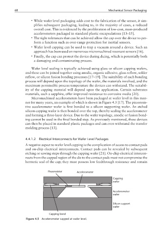
Micromachined accelerometers have been packaged at wafer level in this man-
ner for many years, an example of which is shown in Figure 4.5 [17]. The piezoresis-
tive accelerometer wafer is first bonded to a silicon supporting wafer. An etched
silicon capping wafer is then bonded over the top, thereby sealing the accelerometer
and forming a three-layer device. Due to the wafer topology, anodic or fusion bond-
ing cannot be used in the final bonded step. As previously mentioned, these devices
can then be placed in standard plastic packages and can even withstand the transfer
molding process [13].
4.4.1.2 Electrical Interconnects for Wafer Level Packages
A negative aspect to wafer level capping is the complication of access to contact pads
and on-chip electrical interconnects. Contact pads can be revealed by subsequent
etching or sawing steps through the capping wafer [21]. On-chip electrical intercon-
nects from the capped region of the die to the contact pads must not compromise the
hermetic seal of the cap; they must possess low feedthrough resistance and remain
Piezoresistor Accelerometer
Capping
wafer
Accelerometer
wafer
Silicon support
wafer
Capping bond
Figure 4.5 Accelerometer capped at wafer level.