
Page 80 - MEMS Mechanical Sensors
P. 80
4.4 MEMS Mechanical Sensor Packaging 69
electrically isolated from each other. Techniques for achieving such electrical inter-
connects include [10]:
• P-n junction feedthrough;
• Buried electrode feedthrough;
• Sealed feedthrough channels;
• Thermomigration of aluminum.
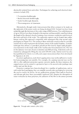
Alternatively, through-wafer interconnects that allow contacts to be made on
the underside of the sensor wafer are being developed [22]. Vertical vias have been
etched through the thickness of the wafer using a DRIE process. Vias with diameters
of up to 200 µm have been formed in this manner and successfully metallized along
the length of the channel, thereby forming a low resistance conductive path between
the front and back of the wafer. The underside contacts can be formed into solder
bumps making this approach compatible with subsequent flip chip second order
packaging (see Figure 4.6). The sealing of these underside contacts must be carefully
carried out in order to preserve the hermetic nature of the sealed chamber. A similar
technique that utilizes a 2-µm-thick polysilicon film heavily doped with phospho-
rous deposited on the inside walls of the vias has also been presented [23]. The vias
in this instance were just 20 µm in diameter and 400 µm long. A hermetic seal was
insured by subsequently filling the vias with LPCVD oxide. Similar work has also
been published by Chow et al. [24], and copper interconnects have been developed
by Nguyen et al. [25].
In certain applications, wafer level capping alone may not be sufficient or wafer
level processing may not suitable. For example, the capping material may not be
able to offer sufficient protection against corrosive media. In these instances, the
capped sensor can be coated in a protective layer or the second order package must
isolate and seal the device.
Protective coatings have been developed for a number of applications, and as
with wafer level packaging, they can simplify second order packaging by removing
the need to isolate the device. In wet applications polymer films such as Parylene
and silicone gels have been successfully employed [26]. Despite the absorption of
water molecules by these polymers, the adhesion of the film to the sensor prevents
Cap
Passivation
Bond
Sensor substrate
Solder bump
Cavity Metal
Vias
Figure 4.6 Through-wafer contacts. (After: [22].)