
Page 85 - MEMS Mechanical Sensors
P. 85
74 Mechanical Sensor Packaging
applied to the diaphragm itself but also to the exposed surfaces of the intermediate
[38]. The resulting stresses induced in the intermediate will be transmitted in part to
the sensing elements and will therefore contribute in some manner to the sensor
output. The magnitude of the effect will depend upon the particular design and the
application. Differential pressure sensing is another example application where this
effect can be important, especially when attempting to detect small differential
pressures imposed on high line pressures. Comprehensive modeling of the assemble
sensor diaphragm and the first order packaging can be used in the design stage to
predict this effect.
4.4.3.2 Mechanical Decoupling
Mechanical decoupling in the form of stress-relieving flexible regions may be incor-
porated on either the sensor or intermediate chip. The flexible regions take the form
of micromachined corrugations that absorb stresses rather than transmit them to the
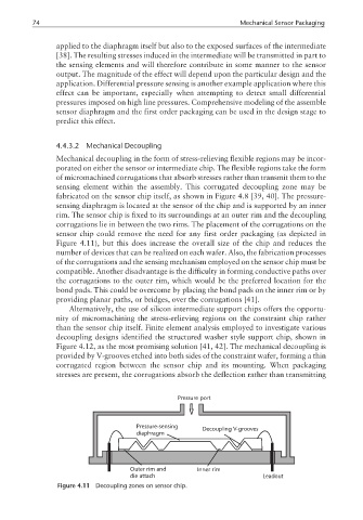
sensing element within the assembly. This corrugated decoupling zone may be
fabricated on the sensor chip itself, as shown in Figure 4.8 [39, 40]. The pressure-
sensing diaphragm is located at the sensor of the chip and is supported by an inner
rim. The sensor chip is fixed to its surroundings at an outer rim and the decoupling
corrugations lie in between the two rims. The placement of the corrugations on the
sensor chip could remove the need for any first order packaging (as depicted in
Figure 4.11), but this does increase the overall size of the chip and reduces the
number of devices that can be realized on each wafer. Also, the fabrication processes
of the corrugations and the sensing mechanism employed on the sensor chip must be
compatible. Another disadvantage is the difficulty in forming conductive paths over
the corrugations to the outer rim, which would be the preferred location for the
bond pads. This could be overcome by placing the bond pads on the inner rim or by
providing planar paths, or bridges, over the corrugations [41].
Alternatively, the use of silicon intermediate support chips offers the opportu-
nity of micromachining the stress-relieving regions on the constraint chip rather
than the sensor chip itself. Finite element analysis employed to investigate various
decoupling designs identified the structured washer style support chip, shown in
Figure 4.12, as the most promising solution [41, 42]. The mechanical decoupling is
provided by V-grooves etched into both sides of the constraint wafer, forming a thin
corrugated region between the sensor chip and its mounting. When packaging
stresses are present, the corrugations absorb the deflection rather than transmitting
Pressure port
Pressure-sensing
Decoupling V-grooves
diaphragm
Outer rim and Inner rim
die attach Leadout
Figure 4.11 Decoupling zones on sensor chip.