
Page 407 -
P. 407
6-16 MEMS: Design and Fabrication
200 µm
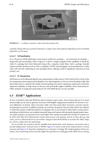
FIGURE 6.13 A multilayer capacitor co-fabricated with package walls.
materials (along with one sacrificial material) on a given layer, three selective depositions and one blanket
deposition can be used.
6.3.6.2 Self-packaging
As a 3-D process, EFAB technology can be used to cofabricate a package — or at least part of a package —
along with and surrounding a device. Figure 6.13 shows a simple example of this capability, in which the
walls of a package have been fabricated along with a capacitor inside them. Such a package typically
requires another element, such as a lid, to complete it. EFAB “self-packaging” can be performed at a wafer
scale, with each die containing its own packaged device, offering a path to significant reduction in total
product cost.
6.3.6.3 IC Integration
EFAB devices can be fabricated directly onto semiconductor wafers such as CMOS and GaAsbyvirtue of the
low-temperature processing involved.Benefits of on-chip integration vs.the use of wire bonding or flip-chip
interconnection to a separate die include reduced package size; lower capacitance, inductance, and noise;
improved scalability to large arrays of devices; and, potentially, higher reliability (fewer interconnects).
Other methods of integrated semiconductor die with EFAB devices are also possible.
6.4 EFAB™ Applications
By now it should be clear that EFAB has almost arbitrary aspect ratios. Tens of layers that are 10 or more
microns high can be used to generate structures with heights ranging from hundreds of microns to sev-
eral millimeters, if desired. These structures, taller even than many LIGA structures, can have micron-
level geometric precision in different patterns on each layer. In general, this procedure allows for mixtures
of scales that operate outside the intuition of a designer who is accustomed to either bulk or surface micro-
machining. Inertial devices can combine extremely large proof masses with extremely densely packed capac-
itor plates; actuators can generate forces much higher than usually associated with MEMS; RF-systems can
be built with fully three-dimensional coaxial interconnects and passives; and all of these devices, and
more, can be co-fabricated next to one another. Designers have the flexibility to consider the“ideal”shape
for a device, rather than the usual shape.
Let us consider the actuation density available from electrostatic comb actuators, commonly used to
provide displacement-invariant force in MEMS. Figure 6.14 shows comb drives implemented in various
processes and Figure 6.15 shows the resulting force as a function of voltage. The implementations shown are:
surface micromachining, which has little depth but typically very small gaps; bulk DRIE silicon etching,
© 2006 by Taylor & Francis Group, LLC