
Page 410 -
P. 410
EFAB™ Technology and Applications 6-19
reduce compliancetowiden sense range or provide more robust structures. The more complex construc-
tions available also enable additional features such as self-test or local monitoring of induced stress to
compensate the device.
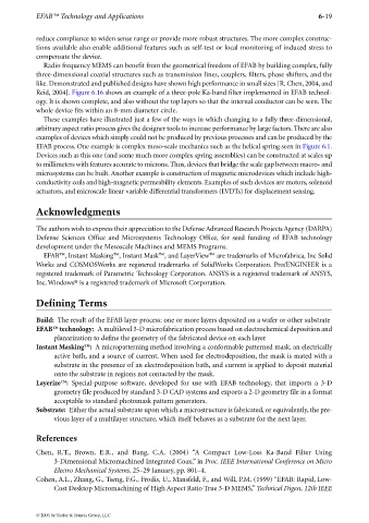
Radio frequency MEMS can benefit from the geometrical freedom of EFAB by building complex, fully
three-dimensional coaxial structures such as transmission lines, couplers, filters, phase shifters, and the
like. Demonstrated and published designs have shown high performance in small sizes [R. Chen, 2004, and
Reid, 2004]. Figure 6.16 shows an example of a three-pole Ka-band filter implemented in EFAB technol-
ogy. It is shown complete, and also without the top layers so that the internal conductor can be seen. The
whole device fits within an 8-mm diameter circle.
These examples have illustrated just a few of the ways in which changing to a fully three-dimensional,
arbitrary aspect ratio process gives the designer tools to increase performance by large factors. There are also
examples of devices which simply could not be produced by previous processes and can be produced by the
EFAB process. One example is complex meso-scale mechanics such as the helical spring seen in Figure 6.1.
Devices such as this one (and some much more complex spring assemblies) can be constructed at scales up
to millimeters with features accurate to microns. Thus, devices that bridge the scale gap between macro- and
microsystems can be built. Another example is construction of magnetic microdevices which include high-
conductivity coils and high-magnetic permeability elements. Examples of such devices are motors, solenoid
actuators, and microscale linear variable differential transformers (LVDTs) for displacement sensing.
Acknowledgments
The authors wish to express their appreciation to the Defense Advanced Research Projects Agency (DARPA)
Defense Sciences Office and Microsystems Technology Office, for seed funding of EFAB technology
development under the Mesoscale Machines and MEMS Programs.
EFAB™, Instant Masking™, Instant Mask™, and LayerView™ are trademarks of Microfabrica, Inc Solid
Works and COSMOSWorks are registered trademarks of SolidWorks Corporation. Pro/ENGINEER is a
registered trademark of Parametric Technology Corporation. ANSYS is a registered trademark of ANSYS,
Inc. Windows® is a registered trademark of Microsoft Corporation.
Defining Terms
Build: The result of the EFAB layer process: one or more layers deposited on a wafer or other substrate
EFAB™ technology: A multilevel 3-D microfabrication process based on electrochemical deposition and
planarization to define the geometry of the fabricated device on each layer
Instant Masking™: A micropatterning method involving a conformable patterned mask, an electrically
active bath, and a source of current. When used for electrodeposition, the mask is mated with a
substrate in the presence of an electrodeposition bath, and current is applied to deposit material
onto the substrate in regions not contacted by the mask.
Layerize™: Special-purpose software, developed for use with EFAB technology, that imports a 3-D
geometry file produced by standard 3-D CAD systems and exports a 2-D geometry file in a format
acceptable to standard photomask pattern generators.
Substrate: Either the actual substrate upon which a microstructure is fabricated, or equivalently, the pre-
vious layer of a multilayer structure, which itself behaves as a substrate for the next layer.
References
Chen, R.T., Brown, E.R., and Bang, C.A. (2004) “A Compact Low-Loss Ka-Band Filter Using
3-Dimensional Micromachined Integrated Coax,” in Proc. IEEE International Conference on Micro
Electro Mechanical Systems, 25–29 January, pp. 801–4.
Cohen, A.L., Zhang, G., Tseng, F.G., Frodis, U., Mansfeld, F., and Will, P.M. (1999) “EFAB: Rapid, Low-
Cost Desktop Micromachining of High Aspect Ratio True 3-D MEMS,” Technical Digest, 12th IEEE
© 2006 by Taylor & Francis Group, LLC