
Page 414 -
P. 414
Single-Crystal Silicon Carbide MEMS: Fabrication, Characterization, and Reliability 7-3
The basic fabrication principles of single-crystal silicon carbide are presented in Section 7.2, in which
SiC device fabrication by photoelectrochemical etching (PECE) and conventional electrochemical etching
(ECE) are discussed. Important etching parameters leading to the fabrication of resistor and diaphragm
structures for sensing applications are also discussed in this section. Relevant SiC fabrication processes
using more recently developed deep reactive ion etching (DRIE) are discussed in another chapter, hence
they will only be discussed here in context. In strain sensor technology, the output of the device is pri-
marily the function of the gauge factor (GF) and resistance. Section 7.3 will discuss the characterization
of SiC GF and resistance, and their temperature dependencies. Contact metallization that is stable at the
desired operating temperature is recognized as critical for successful implementation of high-temperature
sensors. A successful approach to realizing thermally stable ohmic contacts to SiC electronics and sensors
is presented in Section 7.4, along with the deleterious effects of oxygen. Section 7.5 discusses sensor test-
ing and performance characteristics, and finally, Section 7.6 will present the most recent reliability evalu-
ation of SiC pressure sensors that were fabricated using the DRIE process [Beheim and Salupo, 2000],
improved metallization, and packaging.
7.2 Photoelectrochemical Fabrication of 6H-SiC
The difference between PECE and ECE is basically the photo-generation of electron–hole pairs (EHPs)
that occurs during the application of the former. The ECE process is a conventional anodization process
in which high voltage or current is applied to etch away material. In both cases, the etched substrate acts
as the anode electrode. The PECE process is adopted where shallow and anisotropic etching is critical. For
example, in the PECE of resistors, it is important to minimize isotropic etching in order to maintain uni-
form resistor geometry with minimum undercutting across the wafer. Nonuniform geometry of the resis-
tors typically leads to increased circuit imbalance if configured in the Wheatstone bridge form, and
reproducibility becomes difficult.
Unlike silicon technology, processes associated with the fabrication of deep structures in single-crystal
SiC are limited generally to ECE and DRIE. This situation is the result of the near–inert surface chemistry of
SiC that makes conventional wet chemical etching tenuous at room temperature. The fabrication of piezore-
sistor-based sensors in single-crystal SiC requires at least one intentionally doped epilayer, usually n-type, in
which the sensing element is fabricated; this epilayer is grown on a p-type substrate in which the cavity is
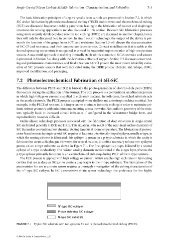
fabricated to create a diaphragm. However, for several reasons, it is often necessary to have two epilayers
grown on an n-type substrate, as shown in Figure 7.1. The first epilayer is p-type, followed by a second
epilayer of n-type conductivity. The resistor sensing elements are fabricated in the n-type layer, whereas the
p-type epilayer primarily functions as an electrochemical etch-stop during PECE of the n-type resistors.
The ECE process is applied with high voltage or current, which enables high etch rates in fabricating
cavities that are as deep as 200µm to create a diaphragm in the n-type substrate. The fabrication of the
piezoresistor for use as a strain sensor requires a thorough investigation of the etching characteristics of
the n -type SiC epilayer. In SiC piezoresistive strain sensor technology, the preference for the highly
+
N -type SiC epilayer
P-type etch-stop SiC epilayer
N-type SiC substrate
FIGURE 7.1 Typical SiC substrate with two epilayers for use in photoelectrochemical etching (PECE).
© 2006 by Taylor & Francis Group, LLC