
Page 418 -
P. 418
Single-Crystal Silicon Carbide MEMS: Fabrication, Characterization, and Reliability 7-7
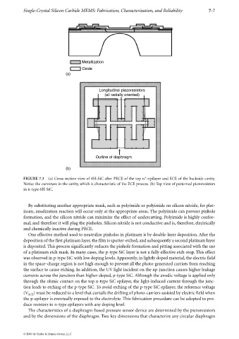
Metallization
Oxide
(a)
Longitudinal piezoresistors
(all radially oriented)
Outline of diaphragm
(b)
FIGURE 7.3 (a) Cross section view of 6H-SiC after PECE of the top n -epilayer and ECE of the backside cavity.
Notice the curvature in the cavity, which is characteristic of the ECE process. (b) Top view of patterned piezoresistors
in n-type 6H-SiC.
By substituting another appropriate mask, such as polyimide or polyimide on silicon nitride, for plat-
inum, anodization reaction will occur only at the appropriate areas. The polyimide can prevent pinhole
formation, and the silicon nitride can minimize the effect of undercutting. Polyimide is highly confor-
mal, and therefore it will plug the pinholes. Silicon nitride is not conductive and is, therefore, electrically
and chemically inactive during PECE.
One effective method used to neutralize pinholes in platinum is by double-layer deposition. After the
deposition of the first platinum layer, the film is sputter-etched, and subsequently a second platinum layer
is deposited. This process significantly reduces the pinhole formation and pitting associated with the use
of a platinum etch mask. In many cases, the p-type SiC layer is not a fully effective etch-stop. This effect
was observed in p-type SiC with low doping levels. Apparently, in lightly doped material, the electric field
in the space–charge region is not high enough to prevent all the photo-generated carriers from reaching
the surface to cause etching. In addition, the UV light incident on the np-junction causes higher leakage
currents across the junction than higher-doped, p-type SiC. Although the anodic voltage is applied only
through the ohmic contact on the top n-type SiC epilayer, the light-induced current through the junc-
tion leads to etching of the p-type SiC. To avoid etching of the p-type SiC epilayer, the reference voltage
(V SCE ) must be reduced to a level that curtails the drifting of photo-carriers assisted by electric field when
the p-epilayer is eventually exposed to the electrolyte. This fabrication procedure can be adopted to pro-
duce resistors in n-type epilayers with any doping level.
The characteristics of a diaphragm-based pressure sensor device are determined by the piezoresistors
and by the dimensions of the diaphragm. Two key dimensions that characterize any circular diaphragm
© 2006 by Taylor & Francis Group, LLC