
Page 416 -
P. 416
Single-Crystal Silicon Carbide MEMS: Fabrication, Characterization, and Reliability 7-5
Hillocks between 10 µm and 50µm formed randomly on the diaphragm surface. The presence of uncon-
trollable discontinuities of this size results in nonuniform stress distributions that adversely affect the
operation of a sensor. Although the cause of the hillock formation was not conclusively determined, there
was evidence that the formations were associated with bubbles generated during the high-rate etching.
The existence of micropipes in the SiC wafers, which could lead to high current–density concentrations
in localized areas, could result in selectively high etch rates around the defect sites, increasing the possi-
bility of etch pit formation. Although the etching potential of highly doped n-type SiC using the ECE
process is much higher than that of p-type SiC, it is possible to stop the etching process at the np-
junction if the ohmic contact used for anodization potential control is made only to the n -SiC epilayer
(refer to Figure 7.1). The positive anodic potential on the n -SiC layer will cause the junction to be
+
reverse-biased, thereby preventing the flow of current through the underlying p-SiC epilayer. In order for
the etch-stop to be effective, the breakdown voltage of the np-junction must be higher than the etching
potential of the n -SiC epilayer. Also, the p-type layer should have a doping level significantly lower than
that of the n -SiC epilayer to minimize the possibility of tunneling current [Shor et al., 1993].
The process of using PECE of SiC for the purpose of fabricating well-defined resistor structures is
described as follows. As shown in Figure 7.1, the starting wafer is an n-type 6H-SiC substrate upon which
3
18
a 5-µm thick, lightly doped (3 10 cm ) p-type epilayer is grown by CVD, followed by a 2µm thick
n -type 6H-SiC epilayer. An ohmic contact metallization, preferably nickel, is deposited and patterned
into a circular shape on the top n -SiC epilayer to enable control of the anodization potential during the
PECE process. Platinum is sputtered onto the top of the wafer, covering the ohmic contact metal and the
entire n -SiC epilayer. The platinum in direct contact with the epilayer is then patterned into the shape of
serpentine resistor elements. This platinum acts as an etch mask, so that the serpentine resistor patterns
can be transferred onto the n -SiC during the PECE process. Contact electrode wire is wire-bonded on
the section of the platinum mask that is in direct contact with the nickel ohmic contact. A thin layer of
black wax is then applied over areas covered by the ohmic contact electrode. The wafer is then immersed
in dilute HF electrolyte, with the side to be etched facing up. This face is then exposed to a UV light
source, with the anodization potential set at 1.7V (SCE means Standard Calomel Electrode, which is
SCE
the reference electrode against which the anode voltage is measured). Under this condition, the exposed
sections of the n -SiC epilayer are photoelectrochemically etched, and the sections under the serpentine-
shaped platinum etch mask are unetched. After the anodization process, the wax is stripped in acetone
and the platinum mask and nickel ohmic contacts are stripped in aqua regia and nitric-hydrochloric acid
in a 50:50 mixture, respectively. After stripping, the resistor patterns transferred to the n epilayer are
revealed.
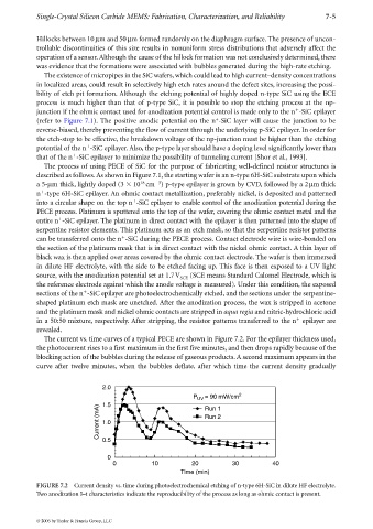
The current vs. time curves of a typical PECE are shown in Figure 7.2. For the epilayer thickness used,
the photocurrent rises to a first maximum in the first five minutes, and then drops rapidly because of the
blocking action of the bubbles during the release of gaseous products. A second maximum appears in the
curve after twelve minutes, when the bubbles deflate, after which time the current density gradually
2.0
P UV = 90 mW/cm 2
1.5 Run 1
Current (mA) 1.0 Run 2
0.5
0
0 10 20 30 40
Time (min)
FIGURE 7.2 Current density vs. time during photoelectrochemical etching of n-type 6H-SiC in dilute HF electrolyte.
Two anodization I–t characteristics indicate the reproducibility of the process as long as ohmic contact is present.
© 2006 by Taylor & Francis Group, LLC