
Page 85 - Mechanical Engineers' Handbook (Volume 2)
P. 85
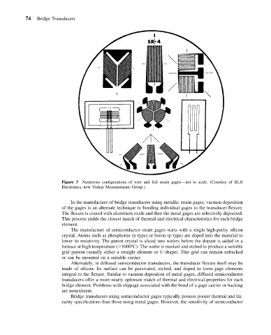
74   Bridge Transducers


                          Figure 3 Numerous configurations of wire and foil strain gages—not to scale. (Courtesy of BLH
                          Electronics, now Vishay Measurements Group.)


                             In the manufacture of bridge transducers using metallic strain gages, vacuum deposition
                          of the gages is an alternate technique to bonding individual gages to the transducer flexure.
                          The flexure is coated with aluminum oxide and then the metal gages are selectively deposited.
                          This process yields the closest match of thermal and electrical characteristics for each bridge
                          element.
                             The manufacture of semiconductor strain gages starts with a single high-purity silicon
                          crystal. Atoms such as phosphorus (n type) or boron (p type) are doped into the material to
                          lower its resistivity. The parent crystal is sliced into wafers before the dopant is added in a
                          furnace at high temperature ( 1000 C). The wafer is masked and etched to produce a suitable
                          grid pattern (usually either a straight element or U-shape). This grid can remain unbacked
                          or can be mounted on a suitable carrier.
                             Alternately, in diffused semiconductor transducers, the transducer flexure itself may be
                          made of silicon. Its surface can be passivated, etched, and doped to form gage elements
                          integral to the flexure. Similar to vacuum deposition of metal gages, diffused semiconductor
                          transducers offer a more nearly optimum match of thermal and electrical properties for each
                          bridge element. Problems with slippage associated with the bond of a gage carrier or backing
                          are nonexistent.
                             Bridge transducers using semiconductor gages typically possess poorer thermal and lin-
                          earity specifications than those using metal gages. However, the sensitivity of semiconductor