
Page 92 - A Practical Guide from Design Planning to Manufacturing
P. 92
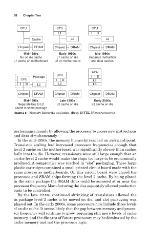
68   Chapter Two


            CPU                CPU               CPU
                                L1               I  D
                  Cache               L2                 L2
           Chipset  DRAM      Chipset  DRAM     Chipset  DRAM

              Mid-1980s         Early 1990s        Mid-1990s
            No on die cache    L1 cache on die  Separate instruction
        L1 cache on motherboard  L2 on motherboard  and data caches


                                                  CPU
                               CPU
                  Package                        I  D
            CPU                I  D               L2
            I  D     L2         L2                L3

           Chipset  DRAM      Chipset  DRAM     Chipset  DRAM
              Mid-1990s          Late 1990s        Early 2000s
           Separate bus to L2  L2 cache on die   L3 cache on die
         cache in same package
        Figure 2-8 Memory hierarchy evolution. (Brey, INTEL Microprocessors.)


        performance mainly by allowing the processor to access new instructions
        and data simultaneously.
          In the mid-1990s, the memory hierarchy reached an awkward point.
        Transistor scaling had increased processor frequencies enough that
        level 2 cache on the motherboard was significantly slower than caches
        built into the die. However, transistors were still large enough that an
        on-die level 2 cache would make the chips too large to be economically
        produced. A compromise was reached in “slot” packaging. These large
        plastic cartridges contained a small printed circuit board made with the
        same process as motherboards. On this circuit board were placed the
        processor and SRAM chips forming the level 2 cache. By being placed
        in the same package the SRAM chips could be accessed at or near the
        processor frequency. Manufacturing the dies separately allowed production
        costs to be controlled.
          By the late 1990s, continued shrinking of transistors allowed the
        in-package level 2 cache to be moved on die, and slot packaging was
        phased out. In the early 2000s, some processors now include three levels
        of on-die cache. It seems likely that the gap between memory and proces-
        sor frequency will continue to grow, requiring still more levels of cache
        memory, and the die area of future processors may be dominated by the
        cache memory and not the processor logic.