
Page 43 - Multifunctional Photocatalytic Materials for Energy
P. 43
32 Multifunctional Photocatalytic Materials for Energy
nanostructures embedded in WO 3 may act as a reflector and light scatterer upon irra-
diating the photoanode from the solution side [44].
A comparison of J/V curves for the photoanode with surface-anchored Au–
3−
PMo 12 O 40 nanoparticles and for bare WO 3 revealed that, in the former case, the
onset potential was less positive by ca. 50 mV and the photocurrent plateau was ap-
proximately twice higher. This very favorable improvement was traced back to the
synergistic combination of various phenomena: (i) a direct catalytic effect of POM-
capped Au NPs in the H 2 O oxidation reaction, taking also into account that the photo-
activity improvement was lower for embedded Au NPs; (ii) local SPR-induced effects
of the Au NPs; and (iii) a buffer action of the polyoxomolybdate layer capping Au
NPs, a phenomenon preventing detrimental recombination processes at WO 3 surface
[41,44].
3.3.3 ZnO-based materials
ZnO, an n-type transparent semiconductor with a high carrier mobility, has been
extensively explored as a photoelectrode for PEC water splitting, thanks to its low
cost and nontoxicity [26,27,53,59,98–101]. Nonetheless, its photoactivity is lim-
ited by its band gap (E G = 3.4 eV) [52,102–107], constraining light absorption to
the UV interval [28,106,108–113] and by the rapid charge carrier recombination
[62,99,102,104,105,114]. To circumvent these difficulties, a considerable attention
has been dedicated to ZnO-based nanosystems, thanks to the possibility of short-
ening the photocarrier diffusion length exploiting the high surface-to-volume ratio.
Unfortunately, the large grain boundary content of nanostructured photoelectrodes
worsens the recombination losses and, at the same time, lowers the electron trans-
port rate [25,26]. To tackle these obstacles and improve photoefficiency, efforts have
been focused on the development of highly crystalline nanowire arrays, that offer
the two-fold advantage of a lower grain boundary content (enhancing hole diffu-
sion) and a fast electron transport perpendicular to the charge-collecting substrate
[16,27]. In this regard, a viable alternative is offered by the use of branched 1D arrays
that also display an improved light harvesting capability due to an effective internal
scattering of the incoming radiation. In particular, an elegant example is offered by
Chen et al. [25], who proposed a two-step hydrothermal route for the preparation of
single- crystalline branched 1D systems through the epitaxial growth of ZnO nano-
disks (NDs) on ZnO nanowire (NWs) arrays. XRD patterns indicated that the only
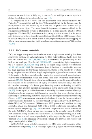
crystalline phase was hexagonal ZnO, with a <001> preferential orientation. The
overall system morphology (Fig. 3.8A) revealed the presence of lateral branches on
the main ZnO NWs, whose surface was coarsened by the secondary growth of ZnO
NDs characterized by a narrow size distribution. The ordered protruding NDs had a
laminated structure and grew perpendicularly with respect to the main NW growth
direction (Fig. 3.8B), inducing a beneficial surface area increase (of ≈70%) with
respect to the pristine NWs [25].
ZnO NWs/NDs were tested as photoanodes for PEC water splitting against a ZnO
NW reference sample (Fig. 3.8C), yielding a significantly higher photocurrent density