
Page 116 - Nanotechnology an introduction
P. 116
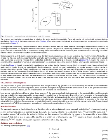
Figure 10.1 An example of a materials selection chart used in classical engineering design at the macroscale.
  The engineer working in the nanoscale has, in principle, far vaster possibilities available. These will only be fully realized with bottom-to-bottom
  nanofacture (Section 8.3), but even nanocomposites (Section 6.5) greatly expand the typically small region occupied by classical composites in
  diagrams like Figure 10.1.
  As components become very small, the statistical nature inherent in present-day “top–down” methods (including the fabrication of a composite by
  blending nanoparticles into a polymer matrix) becomes more apparent. Ultraprecision engineering mostly achieves its high machining accuracy by
  rigorous control of the distributions of control errors making additive contributions to the final result, but ultimate nanoprecision is only achievable
  within a eutactic environment, via bottom-to-bottom nanofacture.
  Similar arguments apply to semiconductor processing. Standard semiconductor devices depend on doping (i.e., the introduction of impurities or
  defects into the pure, perfect semiconductor) for setting the controlling framework for the mobile electron population. The doping level is typically
  quite low, hence as working volumes shrink a statistical distribution of dopants is no longer adequate (Section 10.3). Again,  the  solution  is
  assembly within a eutactic environment, in which each dopant can be placed in a position precisely defined with respect to atomic coordinates.

  Charts like Figure 10.1 really only deal with quantities that are scalars; that is, they can be quantified on a straightforward linear or logarithmic
  scale, such as density. Anisotropic materials with direction-dependent moduli, electrical conductivities, etc. require separate charts according to
  the orientation of the material. Esthetic qualities are not even considered because of their complexity. Even color requires three dimensions; other
  attributes such as “feel” are more difficult still; indeed there is still no standard way of representing them. Yet the history of technology starting from
  the earliest known man-made artifacts shows that purely decorative objects designed to be appreciated esthetically have always preceded objects
  of utility, including weapons and tools, and even entities of a strongly utilitarian nature (such as a motor car) are often chosen on the basis of
  esthetic attributes, provided the minimum requirements of the utility function are met. This must be borne in mind by the designer working in the
  nanoworld.
  10.3. Defects in Nanograins
  The simplest kinds of grains (nanoparticles) are made from a single material, e.g. germanium or silicon. Generally the only issues are whether the
  surface has a different chemical composition, either due to the adsorption of impurities from the environment or due to the generation of lattice
  defects at the surface. In the bulk, the two kinds of defects are vacancies and interstitial ions.
  In compound materials, formed from a cation C and an anion A, the occurrence of defects is governed by the constraint of the need to maintain
  electrical neutrality; i.e., vacancies must be compensated by interstitial ions of the same sign (Frenkel type) or by vacancies of the opposite sign
  (Schottky type). More specifically, they may be cations on interstitial sites and vacancies in the cation half-lattice (Frenkel) or anions on interstitial
  sites and vacancies in the anion half-lattice (anti-Frenkel); cations and anions on interstitial sites (anti-Schottky) or vacancies in the cation and
  anion half-lattices (Schottky). Compounds can be created deliberately non-stoichiometric; e.g., by growth of a granular metal oxide film via physical
  vapor deposition (PVD) in an oxygen-poor atmosphere, thereby assuring an abundance of defects.

  Notation (Schottky)
  The superscript represents the electrical charge of the defect, relative to the undisturbed, overall electrically neutral lattice: ′, ▪, × represent negative,
  positive and neutral (zero) excess electrical charge. Subscript □ is a vacancy, subscript ° is an interstitial. Hence    is an interstitial cation, and
  is a cation vacancy, ‘null’ signifies the undisturbed lattice, and CA represents the addition (at the surface of the nanoparticle) of a new lattice
  molecule. A filled circle is used to represent the substitution of a native ion by a foreign one, e.g.,    would be a divalent cation X on a cation
  lattice site,    would be (mono)valent copper on a silver lattice site in (say) AgCl, etc.

  Relations between Defects
  The following relations are possible [17]


                                                                                                                     (10.1a)

                                                                                                                     (10.1b)

                                                                                                                     (10.1c)