
Page 112 - Nanotechnology an introduction
P. 112
9.3. Carbon Nanoparticles (Fullerenes)
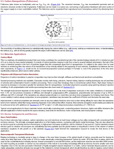
Fullerenes (also known as buckyballs) exist as C , C , etc. (Figure 9.6). The canonical structure, C , has iscosahedral symmetry and an
60
60
70
electronic structure similar to that of graphene. Fullerenes can be made in a carbon arc, but burning a hydrocarbon feedstock with strict control of
the oxygen supply is a more controllable method. The fullerenes can be separated from coproduced soot (“amorphous carbon”) by dissolving them
out.
Figure 9.6 The structure of buckminsterfullerene, C 60 . Note the presence of both hexagons and pentagons. Reproduced with permission from [9].
The possibility of modifying fullerenes by substitutionally doping the carbon lattice (e.g., with boron), adding an endohedral atom, or functionalizing
the surface (e.g., with an amine) greatly expands the ways in which fullerenes can be used [34].
9.4. Materials Applications
Carbon Black
This is a relatively old-established product that even today constitutes the overwhelming bulk of the nanotechnology industry (if it is included as part
of it, as is done by many market analysts). It consists of carbon particles ranging in size from a few to several hundred nanometers; the bulk of the
mass is therefore present in the form of particles bigger than the consensual upper limit of nanoparticles. It is added to the rubber tires for road
vehicles as reinforcing filler; the volume of its manufacture is thus directly related to the popularity of such vehicles. Substitution by fullerene (its true
nano equivalent), cf. Figure 1.3, would not be an economical proposition (except perhaps in Formula 1), even if the properties of the tires were
significantly enhanced, which seems rather unlikely.
Polymers with Dispersed Carbon Nanotubes
Dispersion of carbon nanotubes in polymer composites may improve their strength, stiffness and thermal and electrical conductivities.
Several processing methods are available. Examples include melt mixing, extrusion, internal mixing, injection molding techniques are all used free
of solvents and contamination found in solution processing. There is less fiber breakage than in conventional carbon fibers. High shear mixing is
required as increase in viscosity is greater for nanotubes than for nanoparticles. Controlled alignment is possible using spinning extrusion injection
moulding. In situ polymerization and solution processing have also been used (cf. Section 6.5.1).
The strength improvement depends on the degree of load transfer and on the level of dispersion achieved in the matrix. Additions of nanotubes
from 1–5% vol can produce increases in stiffness and strength in polypropylene (PP), polystyrene, polycarbonate and epoxies of up to 50% in
stiffness and 20% in strength. If the nanotubes are aligned perpendicular to a crack they can slow down propagation by bridging crack faces. This
occurs notably in carbon epoxy composites. In some polymers, nanotubes may decrease the coefficient of friction and decrease the wear rate.
Improvements in electrical properties are dramatic even at very low volume fractions since due to their strong affinity for each other the nanotubes
tend to form networks rather than being randomly dispersed. Even without that effect, however, their extreme elongation would enable percolation to
be achieved at low vol% additions (cf. Section 3.7). In PP or nylon 1–3 vol% dispersed produce resistivities of 1–100 Ω cm.
Typical current applications for these materials include electrically conducting paint, conducting polymer structures, lighter and stiffer structures (the
ultimate application of which would be the space elevator), heat sinks for electronics, motor components, and smart polymer coatings.
9.5. Device Components and Devices
Nano Field Emitters
Due to their extremely high curvature, carbon nanotubes can emit electrons at much lower voltages (a few volts) compared with conventional field
emission devices. The principle envisaged application is in flat display screens, competing with liquid crystal technology. They are also attractive
as electron guns for scanning electron microscopes, in high-power microwave amplifiers, and for miniature X-ray sources. Carbon nanotube-based
electron guns for electron microscopes are undoubtedly the best available (but the global market is insignificant in terms of the volume of carbon
nanotubes required). In situ growth on a flat substrate (Figure 9.5) might diminish the manipulation required to create the final device in this
application.
Nanocomposite Transparent Electrodes
Display technology is inevitably going to have to change in the near future because of the global dearth of indium, presently used for doping tin
oxide (at a fairly high level, of the order of 10%) to create electrically conducting transparent “indium tin oxide” (ITO) thin films on glass, which are
used as the counterelectrode in display devices. Annual consumption is around 800 tonnes, yet the total known reserves are less than 3000 tonnes.
As much recycling as possible is carried out, but extraction of the indium is becoming increasingly difficult as devices become smaller and more
integrated. Due to the very low percolation threshold of highly elongated objects dispersed in a matrix, carbon nanotube-doped polymers can be
made adequately conductive at levels low enough for the material to remain transparent, which should therefore be able to replace current indium