
Page 136 - Op Amps Design, Applications, and Troubleshooting
P. 136
High-Current Amplifier 119
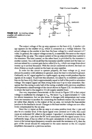
FIGURE 2.32 An inverting voltage
amplifier with additional current
amplification.
The output voltage of the op amp appears on the base of Qj. A similar volt-
age appears on the emitter of Q lf which is connected as a voltage follower. The
actual voltage on the emitter is less than the base voltage by a small amount (=0.7
volts). In general, the output voltage across R L is essentially the same as the output
voltage of the op amp. The output current of the op amp provides base current to
the transistor. The load current, on the other hand, is provided by the transistor's
emitter current. You will recall that the transistor emitter current and the base cur-
rent are related by a current gain factor called j8 or h FE, which can range from about
twenty up to several thousand. With the circuit connected as shown, the load can
draw ft times as much current as the basic op amp supplies.
In order for the circuit to operate properly, the base voltage on Qi must
always be positive with reference to ground, since the load is returned to ground.
Ordinarily, an AC signal applied to a split-supply op amp would produce bipolar
signals on its output. To prevent this situation, we adjust R P to establish a positive
bias on the base of Qj that is approximately equal to half of the positive saturation
voltage. The output signal can then swing from near 0 up to near saturation. Rec-
ognize mat this swing is only half of the swing available with previous amplifiers
and represents a disadvantage of the circuit shown in Figure 2.32. An alternative is
to return the load to the negative 15-volt supply (emitter bias).
One very important characteristic of the circuit in Figure 2.32 is that output
voltage is unaffected by changes in V m. We know V BE is approximately 0.7 volts
for silicon transistors, but we also know it changes with temperature and varies
from one transistor to another. By connecting the feedback resistor (R F) to the emit-
ter rather than directly to the output of the op amp, we include the base-emitter
junction in the feedback circuit. Changes in the base-emitter voltage are now effec-
tively compensated by the op amp.
Since the (+) input on the op amp is at some positive level, the (-) pin will
also be at a similar level. If the input signal were centered on 0 volts, this could
cause an undesired IX offset in the output. Capacitor Q is included to isolate the
DC level on the (-) pin from the DC level associated with the signal source. If it is
sufficiently large, it has no effect on the gain calculations in the circuit. If its reac-
tance at the lowest input frequency exceeds one-tenth the resistance of jR f, then the
gain of the circuit should be computed in the same manner as the AC-coupled
amplifiers discussed in a previous section.