
Page 178 - Op Amps Design, Applications, and Troubleshooting
P. 178
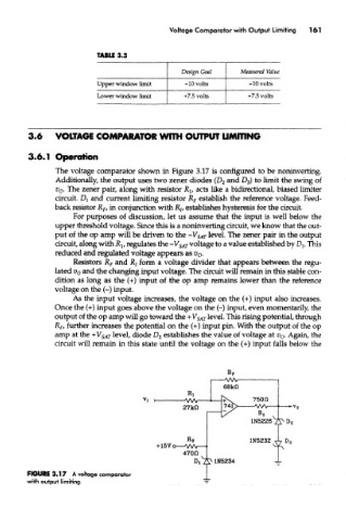
Voltage Comparator with Output Limiting  161


                          TABLE 3.3

                                                 Design Goal     Measured Value
                           Upper window limit     +10 volts        +10 volts
                           Lower window limit     +7.5 volts       +7.5 volts


         L6    VOLTAGE COMPARATOR WITH OUTPUT LIMITING


         1*6.1 Operation
                The voltage comparator shown in Figure 3.17 is configured to be noninverting.
                Additionally, the output uses two zener diodes (D 2 and D 3) to limit the swing of
                v 0. The zener pair, along with resistor Rj, acts like a bidirectional, biased limiter
               circuit. DI and current limiting resistor R s establish the reference voltage. Feed-
               back resistor R F, in conjunction with R It establishes hysteresis for the circuit.
                    For purposes of discussion, let us assume that the input is well below the
               upper threshold voltage. Since this is a noninverting circuit, we know that the out-
               put of the op amp will be driven to the -V SAT level. The zener pair in the output
               circuit, along with RI, regulates the -VSAT voltage to a value established by D 3. This
               reduced and regulated voltage appears as v 0.
                    Resistors R F and R/ form a voltage divider that appears between the regu-
               lated v 0 and the changing input voltage. The circuit will remain in this stable con-
               dition as long as the (+) input of the op amp remains lower than the reference
               voltage on the (-) input.
                    As the input voltage increases, the voltage on the (+) input also increases.
               Once the (+) input goes above the voltage on the (-) input, even momentarily, the
               output of the op amp will go toward the + V SAT level. This rising potential, through
               R F, further increases the potential on the (+) input pin. With the output of the op
               amp at the +V SAT level, diode D 2 establishes the value of voltage at v 0. Again, the
               circuit will remain in this state until the voltage on the (+) input falls below the


        FIGURE 3.17 A voltage comparator               i
        with output limiting.