Page 193 - Op Amps Design, Applications, and Troubleshooting
P. 193
176    OSCILLATORS


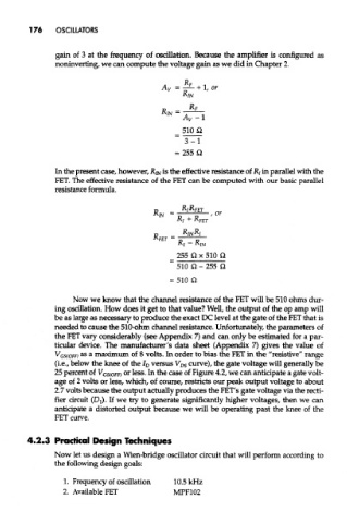
                gain of 3 at the frequency of oscillation. Because the amplifier is configured as
                noninverting, we can compute the voltage gain as we did in Chapter 2.


               In the present case, however, R/^ is the effective resistance of JR/ in parallel with the
               FET. The effective resistance of the FET can be computed with our basic parallel
               resistance formula.


                    Now we know that the channel resistance of the FET will be 510 ohms dur-
               ing oscillation. How does it get to that value? Well, the output of the op amp will
               be as large as necessary to produce the exact "DC level at the gate of the FET that is
               needed to cause the 510-ohm channel resistance. Unfortunately, the parameters of
               the FET vary considerably (see Appendix 7} and can only be estimated for a par-
               ticular device. The manufacturer's data sheet (Appendix 7} gives the value of
               V GS(OFF) as a maximum of 8 volts. In order to bias the FET in the "resistive" range
               (i.e., below the knee of the I D versus V DS curve), the gate voltage will generally be
               25 percent of V GS(OFF) or less. In the case of Figure 4.2, we can anticipate a gate volt-
               age of 2 volts or less, which, of course, restricts our peak output voltage to about
               2.7 volts because the output actually produces the FET's gate voltage via the recti-
               fier circuit (DI). If we try to generate significantly higher voltages, then we can
               anticipate a distorted output because we will be operating past the knee of the
               FET curve.


        4.2.3 Practical Design Techniques

               Now let us design a Wien-bridge oscillator circuit that will perform according to
               the following design goals:

                  1. Frequency of oscillation  10.5 kHz
                  2. Available FET             MPF102

