
Page 198 - Op Amps Design, Applications, and Troubleshooting
P. 198
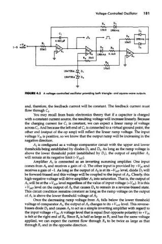
Voltage-Controlled Oscillator  181


               FIGURE 4.5 A voltage-controlled oscillator providing both triangle- and square-wave outputs.


               and, therefore, the feedback current will be constant. The feedback current must
               flow through Q.
                    You may recall from basic electronics theory that if a capacitor is charged
               with a constant current source, the resulting voltage will increase linearly. Because
               the charging current for Q is constant, we can expect a linear ramp of voltage
               across Q. And because the left end of Q is connected to a virtual ground point, the
               other end (output of the op amp) will reflect the linear ramp voltage. The input
               voltage V IN is positive, so we know that the output ramp will be increasing in the
               negative direction.
                    A 2 is configured as a voltage comparator circuit with the upper and lower
               thresholds being established by diodes Dj and D 2. As long as the ramp voltage is
               above the lower threshold point (established by Dt), the output of amplifier A 2
               will remain at its negative limit (-V SAT).
                    Amplifier A 3 is connected as an inverting summing amplifier. One input
               comes from A 2 and receives a gain of -2. The other input is provided by +V !N and
               receives a gain of -1. As long as the output of A 2 is at its -~V SAT level, diode D 3 will
               be forward-biased and this voltage will be coupled to the input of A 3, Clearly, this
               high-negative voltage will drive amplifier A 3 into saturation. That is, the output of
               A 3 will be at the + V SAT level regardless of the value of input voltage (+V^). It is this
               +VSAT level on the output of A 3 that causes D 4 to remain in a reverse-biased state.
               This circuit condition remains constant as long as the ramp voltage on the output
               of AI is above the lower threshold voltage of A 2.
                    Once the decreasing ramp voltage from AI falls below the lower threshold
               voltage of comparator AI, the output of A 2 changes to its +V SAT level. This reverse-
               biases diode D 3 and causes A 3 to act as a simple inverting amplifier with regard to
               the input voltage + V iN. A voltage level that is equal (but opposite polarity) to +V IN
               is felt at the right end of R 4. Since R* is half as large as R a and has the same voltage
               applied, we can expect the current flow through JR 4 to be twice as large as that
               through RI and in the opposite direction.