Page 203 - Op Amps Design, Applications, and Troubleshooting
P. 203
186    OSCILLATORS


                for the -1-volt input case. The input current for the -5-volt case is


                                         j = -T     = 500 jjA
                                          * 4  10 k&

                    Let us consider the electron flow in the case of a 1-volt input. Recall that Rj
               will have a 50-microampere current flowing in a right-to-left direction. R 4, as com-
               puted, will have a current of 100 microamperes flowing from right to left. When
               the latter current gets to the summing point of A lf it splits. One part, 50 microam-
               peres, goes through RI and satisfies the requirements of +V IN and R 5. Kirchhoffs
               Current Law tells us that the remaining 50 microamperes must flow into Q in a
               left-to-right direction. It is very important to note that the magnitude of this charg-
               ing current is identical to that which flowed on the previous alternation, but it is
               flowing in the opposite direction. Therefore, Q will charge at the same rate but in
               the opposite polarity. Because the charging currents are equal and the required
               voltage change (AFci) is the same, the amount of time for this alternation will be
               the same as the first. Given this observation, we can now compute the frequency
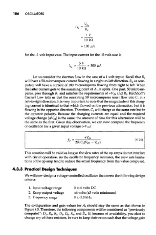
               of oscillation for a given input voltage (+V IN):


               This equation will be valid as long as the slew rates of the op amps do not interfere
               with circuit operation. As the oscillator frequency increases, the slew rate limita-
               tions of the op amp tend to reduce the actual frequency from the value computed.

        4.3.3 Practical Design Techniques
               We will now design a voltage-controlled oscillator that meets the following design
               criteria:
                  1. Input voltage range    0 to 6 volts DC
                  2. Ramp output voltage    ±4 volts (±3 volts minimum)
                  3. Frequency range        0 to 5.0 kHz

               The configuration and gain values for A 3 should stay the same as that shown in
               Figure 4.5. Therefore, the following components will be considered as "previously
               computed": D 3, R 3/ R 5, D 5, D 6, R^ and D 4. If, because of availability, you elect to
               change any of these resistors, be sure to keep their ratios such that the voltage gain

