
Page 207 - Op Amps Design, Applications, and Troubleshooting
P. 207
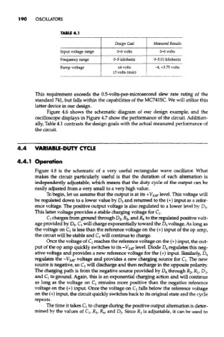
190   OSCILLATORS

                          TABLE 4.1

                                                Design Goal     Measured Results
                          Input voltage range    0-6 volts        0-6 volts
                          Frequency range      0-5 kilohertz    0-5.01 kilohertz
                          Ramp voltage           ±4 volts       -4, +3.75 volts
                                               ±3 volts (min)


               This requirement exceeds the 0.5-volts-per-microsecond slew rate rating of the
               standard 741, but falls within the capabilities of the MC741SC. We will utilize this
               latter device in our design.
                    Figure 4.6 shows the schematic diagram of our design example, and the
               oscilloscope displays in Figure 4.7 show the performance of the circuit. Addition-
               ally, Table 4.1 contrasts the design goals with the actual measured performance of
               the circuit.


        4.4    VARIABLE-DUTY CYCLE

        4.4.1 Operation

               Figure 4.8 is the schematic of a very useful rectangular wave oscillator. What
               makes the circuit particularly useful is that the duration of each alternation is
               independently adjustable, which means that the duty cycle of the output can be
               easily adjusted from a very small to a very high value.
                    To begin, let us assume that the output is at its +VSAT level. This voltage will
               be regulated down to a lower value by D 3 and returned to the (+) input as a refer-
               ence voltage. The positive output voltage is also regulated to a lower level by D 5.
               This latter voltage provides a stable charging voltage for Q.
                    Q charges from ground through D 2, #3, and R 4 to the regulated positive volt-
               age provided by D 5. Q will charge exponentially toward the D 5 voltage. As long as
               the voltage on Q is less than the reference voltage on the (+) input of the op amp,
               the circuit will be stable and Q will continue to charge.
                    Once the voltage of Q reaches the reference voltage on the (+) input, the out-
               put of the op amp quickly switches to its -V SAT level. Diode D 4 regulates this neg-
               ative voltage and provides a new reference voltage for the (+) input. Similarly, D 6
               regulates the -V SAT voltage and provides a new charging source for Q. The new
               source is negative, so Q will discharge and then recharge in the opposite polarity.
               The charging path is from the negative source provided by D 6 through R 2, R lf D l7
               and Q to ground. Again, this is an exponential charging action and will continue
               as long as the voltage on Q remains more positive than the negative reference
               voltage on the (+) input. Once the voltage on Q falls below the reference voltage
               on the (+) input, the circuit quickly switches back to its original state and the cycle
               repeats.
                    The time it takes Q to charge during the positive output alternation is deter-
               mined by the values of Q, R 3, R 4, and D 5. Since R 3 is adjustable, it can be used to