
Page 212 - Op Amps Design, Applications, and Troubleshooting
P. 212
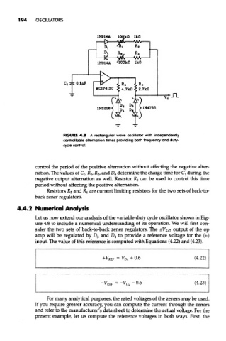
194    OSCILLATORS


                           FIGURE 4.8 A rectangular wave oscillator with independently
                           controllable alternation times providing both frequency and duty-
                           cycle control.


               control the period of the positive alternation without affecting the negative alter-
               nation. The values of Q, R lf R 2, and D 6 determine the charge time for Q during the
               negative output alternation as well. Resistor R } can be used to control this time
               period without affecting the positive alternation.
                    Resistors R 5 and R 6 are current limiting resistors for the two sets of back-to-
               back zener regulators.
        4.4.2 Numerical Analysis

               Let us now extend our analysis of the variable-duty cycle oscillator shown in Fig-
               ure 4.8 to include a numerical understanding of its operation. We will first con-
               sider the two sets of back-to-back zener regulators. The ±V SAT output of the op
               amp will be regulated by D 3 and D 4 to provide a reference voltage for the (+)
               input. The value of this reference is computed with Equations (4.22) and (4.23).


                    For many analytical purposes, the rated voltages of the zeners may be used.
               If you require greater accuracy, you can compute the current through the zeners
               and refer to the manufacturer's data sheet to determine the actual voltage. For the
               present example, let us compute the reference voltages in both ways. First, the