
Page 290 - Op Amps Design, Applications, and Troubleshooting
P. 290
272 POWER SUPPLY CIRCUITS
This high-power dissipation is one major disadvantage of shunt-regulator circuits.
The collector-to-emitter breakdown voltage must be higher than V mG(max).
In the present case, the transistor breakdown rating for V CEO must be greater than
15 volts.
Many transistors will satisfy the requirements of our design. For purposes of
illustration, let us select an MJE2090, which, as the manufacturer's data sheet
(Appendix 2) indicates, is a Darlington power transistor that satisfies all of our
requirements. The calculations presented in Appendix 10 dictate the use of a heat
sink for the transistor.
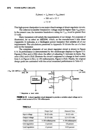
The complete schematic of our shunt regulator circuit is shown in Figure
6.14. Its performance is demonstrated by the oscilloscope displays in Figure 6.15.
Figures 6.15(a) and 6.15(b) show the effect of adjusting ?! between its limits. Fig-
ures 6.15(c) and 6.15(d) illustrate the circuit's response to a change in load current
from 0, in Figure 6.15(c), to 150 milliamperes, Figure 6.15(d). Finally, the original
design goals are contrasted with the actual measured performance in Table 6.3.
* Requires a heat sink
FIGURE 6.14 A shunt regulator circuit designed to provide a variable output voltage and to
supply a load current of 0 to 150 milliamperes
TABU 6.3
Design Goal Measured Value
Input voltage 18-22 volts 18-22 volts
Output voltage 12-15 volts 12.5-15.5 volts
Output current 0-150 milliamperes 0-150 milliamperes
Line regulation <2 percent 0.8 percent
Load regulation <2 percent 0.012 percent