
Page 87 - Op Amps Design, Applications, and Troubleshooting
P. 87
AMPLIFIERS
Since the slew rate of the 741 exceeds this minimum value, we can continue with
our initial op amp selection. If the above calculation indicates a higher require-
ment than our preliminary op amp selection can deliver, then another op amp
must be selected that has a higher slew rate.
Calculate the Value of Compensation Resistor (R B). The compensation
resistor (R B) reduces the error in the output voltage caused by the voltage drops
that result from the op amp's input bias currents. As with the inverting configura-
tion, we achieve maximum error reduction by inserting equal resistances between
both op amp input terminals and ground. The resistance between the inverting
input to ground is essentially equal to the parallel combination of R/ and R F. This
is easier to appreciate if you remember that the output impedance of an op amp is
very low. For purposes of this analysis, assume that the output impedance is actu-
ally 0 ohms. In this condition, one end of both R/ and R f connect to ground and the
other ends connect to the inverting input terminal. Thus, they are effectively in
parallel. The value of R B is calculated as in Equation (2.26):
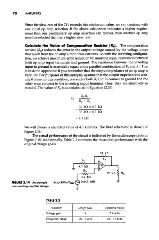
We will choose a standard value of 4.3 kilohms. The final schematic is shown in
Figure 2.14.
The actual performance of the circuit is indicated by the oscilloscope plots in
Figure 2.15. Additionally, Table 2.2 contrasts the measured performance with the
original design goals.
FIGURE 2.14 An example
noninverting amplifier design.
TABLE 2.2
Parameter Design Goal Measured Values
Voltage gain 8 7.9-8.01
Frequency range DC-5 kHz DC->5 kHz