Page 90 - Op Amps Design, Applications, and Troubleshooting
P. 90
Voltage Follower   73


        2.4.2 Numerical Analysis
               The numerical analysis for the voltage follower is simpler than for previous cir-
               cuits because of the lack of circuit complexity. Let us analyze the circuit shown in
               Figure 2.16 and determine the following values:

                  1. Voltage gain
                  2. Input impedance
                  3. Input current requirement
                 4. Maximum output voltage swing
                 5. Slew-rate limiting frequency
                 6. Maximum input voltage swing
                 7. Output impedance
                 8. Output current capability
                 9. Bandwidth
                 10, Power supply rejection ratio

               For purposes of the following analyses, let us assume that the op amp in Figure
               2.16 is a 741.

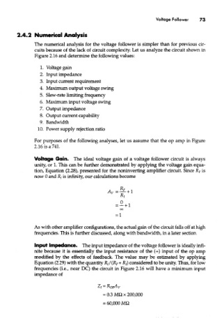
               Voltage Gain. The ideal voltage gain of a voltage follower circuit is always
               unity, or 1. This can be further demonstrated by applying the voltage gain equa-
               tion, Equation (2.28), presented for the noninverting amplifier circuit. Since R F is
               now 0 and R/ is infinity, our calculations become


               As with other amplifier configurations, the actual gain of the circuit falls off at high
               frequencies. This is further discussed, along with bandwidth, in a later section.

               Input Impedance. The input impedance of the voltage follower is ideally infi-
               nite because it is essentially the input resistance of the (+) input of the op amp
               modified by the effects of feedback. The value may be estimated by applying
               Equation (2.29) with the quantity R//(Rf + R/) considered to be unity. Thus, for low
               frequencies (i.e., near DC) the circuit in Figure 2.16 will have a rninimum input
               impedance of

