
Page 95 - Op Amps Design, Applications, and Troubleshooting
P. 95
78 AMPLIFIERS
Now let us check to be sure the 741 can supply the required current to our
load without causing an appreciable voltage loss in our output. When the output
voltage reaches its maximum level, the load current can be computed with Ohm's
Law as
This should have negligible effect on the output voltage of the op amp because the
741 can supply significantly higher currents.
Figure 2.17 also illustrates the use of a compensating resistor R B, Recall from
the previous amplifier designs that bias current in the op amp can cause output off-
sets because of the voltage drops across any resistances in line with the bias cur-
rent. We minimize this offset by providing equal resistances in both (+) and (-)
inputs. The resistance in the (+) input is simply the source resistance that was given
as 1.8 kilohms. To minimize output errors, we insert an equal value R B in the feed-
back loop. Note that no significant signal current flows through Kg. Therefore, the
voltage gain is unaffected by the addition of R s/ and it remains constant at unity.
The actual performance of our voltage follower circuit is shown in Figure
2.18 through the use of an oscilloscope plot. The measured performance is com-
pared to the design goals in Table 2.3.
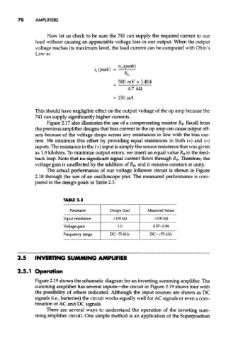
TABLE 2.3
Parameter Design Goal Measured Values
Input resistance >100fcQ >100 kQ.
Voltage gain 1.0 0.97-0.99
Frequency range DC-75 kHz DC->75 kHz
2.5 INVERTING SUMMING AMPLIFIER
2.5.1 Operation
Figure 2.19 shows the schematic diagram for an inverting summing amplifier. The
summing amplifier has several inputs—the circuit in Figure 2.19 shows four with
the possibility of others indicated. Although the input sources are shown as DC
signals (i.e., batteries) the circuit works equally well for AC signals or even a com-
bination of AC and DC signals.
There are several ways to understand the operation of the inverting sum-
ming amplifier circuit. One simple method is an application of the Superposition