
Page 98 - Op Amps Design, Applications, and Troubleshooting
P. 98
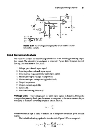
Inverting Summing Amplifier  81


                         FIGURE 2.20  An inverting summing amplifier circuit used for a numer-
                         ical analysis example.


        2.5.2 Numerical Analysis

               We will now analyze the numerical performance of an inverting surriming ampli-
               fier circuit. The circuit to be analyzed is shown in Figure 2.20. Compute the fol-
               lowing characteristics of the circuit:

                  1. Voltage gain of each input signal
                  2. Input impedance of each input signal
                  3. Input current requirement for each input signal
                  4. Maximum output voltage swing (total)
                  5. Maximum input voltage swing (individual)
                  6. Output impedance
                  7. Output current capability
                  8. Bandwidth
                  9. Slew-rate limiting frequency

               Voltage Gain. The voltage gain for each input signal in Figure 2.20 must be
               computed separately. Each gain, however, is computed in the same manner, Equa-
               tion (2.6), as a simple inverting amplifier circuit. That is,


               where the minus sign is used to remind us of the phase inversion given to each
               signal.
                    The individual voltage gains for the circuit in Figure 2.20 are computed: