
Page 100 - Optical Communications Essentials
P. 100
Light Sources and Transmitters
90 Chapter Six
device can be turned on and off by an electric signal to produce a corresponding
optical output pattern. As the next two sections describe, laser diodes can be
modulated significantly faster than LEDs. However, there is a speed limit
beyond which even the laser does not respond fast enough to the changes in an
electric signal. Beyond this point a steady light output stream from the laser
diode is fed into an external device, which can change the intensity of the light
that passes through it very rapidly. This process is known as external modula-
tion. Section 6.5 describes external modulators in greater detail.
6.2. LEDs
If we look around us, we notice LEDs everywhere. They can be seen glowing
green, yellow, or red in vehicles, computer equipment, kitchen appliances, tele-
phones, cameras, and every imaginable piece of electronic equipment. They
are inexpensive and highly reliable light sources. The LEDs used in optical
communications are much smaller and emit in the infrared region, but com-
pared to the other telecommunication light sources used, they are much less
expensive and easier to use in transmitter designs. However, because of their
relatively low power output, broad emission pattern, and slow turn-on time,
their use is limited to low-speed (less than 200-Mbps), short-distance (up to a
few kilometers) applications using multimode fibers.
6.2.1. Principles of operation
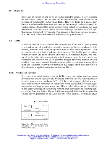
To create a material structure for an LED, n-type and p-type semiconductor
materials are joined together. The boundary between the two joined materials
is called a pn junction, as shown in Fig. 6.2. To create a supply of electrons and
holes that may flow across the pn junction to recombine and thereby emit light,
one applies a voltage across the junction. This is called a bias voltage. Variations
in the applied voltage, or the driving current, then correspond to a varying opti-
cal output from the device. Figure 6.3 shows a typical relationship between the
optical power generated by an LED and the drive current. Nominally LEDs
Figure 6.2. Electrons and holes
recombine at a pn junction and
thereby emit light.
Downloaded from Digital Engineering Library @ McGraw-Hill (www.digitalengineeringlibrary.com)
Copyright © 2004 The McGraw-Hill Companies. All rights reserved.
Any use is subject to the Terms of Use as given at the website.