
Page 98 - Optical Communications Essentials
P. 98
Light Sources and Transmitters
88 Chapter Six
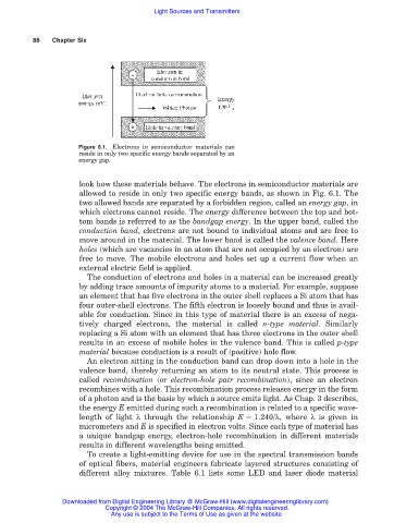
Figure 6.1. Electrons in semiconductor materials can
reside in only two specific energy bands separated by an
energy gap.
look how these materials behave. The electrons in semiconductor materials are
allowed to reside in only two specific energy bands, as shown in Fig. 6.1. The
two allowed bands are separated by a forbidden region, called an energy gap, in
which electrons cannot reside. The energy difference between the top and bot-
tom bands is referred to as the bandgap energy. In the upper band, called the
conduction band, electrons are not bound to individual atoms and are free to
move around in the material. The lower band is called the valence band. Here
holes (which are vacancies in an atom that are not occupied by an electron) are
free to move. The mobile electrons and holes set up a current flow when an
external electric field is applied.
The conduction of electrons and holes in a material can be increased greatly
by adding trace amounts of impurity atoms to a material. For example, suppose
an element that has five electrons in the outer shell replaces a Si atom that has
four outer-shell electrons. The fifth electron is loosely bound and thus is avail-
able for conduction. Since in this type of material there is an excess of nega-
tively charged electrons, the material is called n-type material. Similarly
replacing a Si atom with an element that has three electrons in the outer shell
results in an excess of mobile holes in the valence band. This is called p-type
material because conduction is a result of (positive) hole flow.
An electron sitting in the conduction band can drop down into a hole in the
valence band, thereby returning an atom to its neutral state. This process is
called recombination (or electron-hole pair recombination), since an electron
recombines with a hole. This recombination process releases energy in the form
of a photon and is the basis by which a source emits light. As Chap. 3 describes,
the energy E emitted during such a recombination is related to a specific wave-
length of light λ through the relationship E 1.240/λ, where λ is given in
micrometers and E is specified in electron volts. Since each type of material has
a unique bandgap energy, electron-hole recombination in different materials
results in different wavelengths being emitted.
To create a light-emitting device for use in the spectral transmission bands
of optical fibers, material engineers fabricate layered structures consisting of
different alloy mixtures. Table 6.1 lists some LED and laser diode material
Downloaded from Digital Engineering Library @ McGraw-Hill (www.digitalengineeringlibrary.com)
Copyright © 2004 The McGraw-Hill Companies. All rights reserved.
Any use is subject to the Terms of Use as given at the website.