
Page 355 - Optical Communications Essentials
P. 355
Manufacturing Issues
Manufacturing Issues 345
moves from one side of the module to the other in proportion to the applied volt-
age. Thus, one module face will be cooled while the other is heated simultan-
eously. As noted in Chap. 6, with appropriate control circuitry TE coolers can
stabilize temperatures to 0.02°C.
In packaging devices such as laser diodes, careful design procedures must be
followed to ensure that the heat generated by the laser chip during operation
will flow away from the laser out of the package. Creating the interface between
a laser chip and the carrier it is mounted on is a standard procedure known as
eutectic die attachment. This bonding traditionally is done by means of a
gold/tin solder (80% Au/ 20% Sn), which can be done in a fairly straightforward
manner in an automated assembly environment.
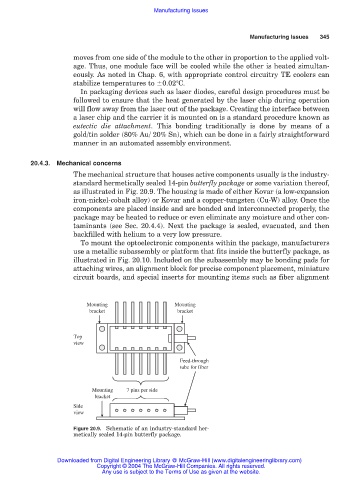
20.4.3. Mechanical concerns
The mechanical structure that houses active components usually is the industry-
standard hermetically sealed 14-pin butterfly package or some variation thereof,
as illustrated in Fig. 20.9. The housing is made of either Kovar (a low-expansion
iron-nickel-cobalt alloy) or Kovar and a copper-tungsten (Cu-W) alloy. Once the
components are placed inside and are bonded and interconnected properly, the
package may be heated to reduce or even eliminate any moisture and other con-
taminants (see Sec. 20.4.4). Next the package is sealed, evacuated, and then
backfilled with helium to a very low pressure.
To mount the optoelectronic components within the package, manufacturers
use a metallic subassembly or platform that fits inside the butterfly package, as
illustrated in Fig. 20.10. Included on the subassembly may be bonding pads for
attaching wires, an alignment block for precise component placement, miniature
circuit boards, and special inserts for mounting items such as fiber alignment
Mounting Mounting
bracket bracket
Top
view
Feed-through
tube for fiber
Mounting 7 pins per side
bracket
Side
view
Figure 20.9. Schematic of an industry-standard her-
metically sealed 14-pin butterfly package.
Downloaded from Digital Engineering Library @ McGraw-Hill (www.digitalengineeringlibrary.com)
Copyright © 2004 The McGraw-Hill Companies. All rights reserved.
Any use is subject to the Terms of Use as given at the website.