
Page 232 - Organic Electronics in Sensors and Biotechnology
P. 232
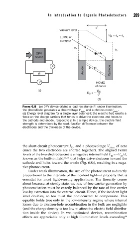
An Intr oduction to Or ganic Photodetectors     209


                                                        d
                                    Vacuum level
                                                                  = f  – f
                                    LUMO of                    V BI  a  c
                                    acceptor
                                            f a                   f

                       OPV                                         c
                      device

                               A
                                                 Anode          Cathode
                        R

                        V                               HOMO
                                                       of donor
                        (a)                             V BI
                                                   E  = –  d
                                                    BI
                                                         (b)
               FIGURE 6.8  (a) OPV device driving a load resistance R; under illumination,
               the photodiode generates a photovoltage V   and a photocurrent I  .
                                               photo             photo
               (b) Energy level diagram for a single-layer solar cell; the electric fi eld exerts a
               force on the charge carriers that tends to drive the electrons and holes to
               the cathode and anode, respectively. In a simple device, the electric fi eld
               strength is determined by the work function difference between the
               electrodes and the thickness of the device.


               the short-circuit photocurrent J , and a photovoltage V  of zero
                                          SC                   photo
               (since the two electrodes are shorted together). The aligned Fermi
               levels of the two electrodes create a negative internal field E =−V /d,
                                                                BI   BI
               known as the built-in field, 44, 45  that helps drive electrons toward the
               cathode and holes toward the anode (Fig. 6.8b), resulting in a nega-
               tive photocurrent.
                   Under weak illumination, the size of the photocurrent is directly
               proportional to the intensity of the incident light––a property that is
               essential for most light-sensing applications. The linearity comes
               about because, at steady state, the rate of free carrier generation by
               photoexcitation must be exactly balanced by the rate of free carrier
               loss by extraction into the external circuit. Hence, if the incident light
               level doubles, so too must the photocurrent to compensate. This
               equality holds true only in the low-intensity regime where internal
               losses due to electron-hole recombination in the bulk are negligible
               (and the charge density is too low to affect the electric field distribu-
               tion inside the device). In well-optimized devices, recombination
               effects are appreciable only at high illumination levels exceeding 46