
Page 399 - Organic Electronics in Sensors and Biotechnology
P. 399
376 Chapter Ten
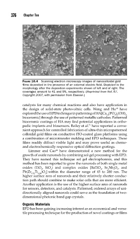
FIGURE 10.4 Scanning electron microscopy images of nanocolloidal gold
fi lms deposited in the presence of an external electric fi eld. Depicted is the
morphology after the deposition experiments shown of left and of right. The
coverages amount to 41 and 9%, respectively. (Reprinted from Ref. 67.
Copyright 2007, with permission from Elsevier.)
catalysts for many chemical reactions and also have application in
40
the design of solid-state photovoltaic cells. Wang and Hu have
explored the use of EPD technique in patterning of HA [Ca (PO ) (OH)
10 3 6 2,
bioceramic] through the use of patterned metallic cathodes. Patterned
bioceramic coatings of HA may find potential applications in ortho-
71
pedic implants and biosensors. Bailey et al. have reported a conve-
nient approach for controlled fabrication of ultra-thin micropatterned
colloidal gold films on conductive ITO-coated glass platforms using
a combination of microtransfer molding and EPD techniques. These
films readily diffract visible light and may prove useful as chemo-
and electrochemically responsive optical diffraction gratings.
44
Limmer and Cao have demonstrated a new method for the
growth of oxide nanorods by combining sol-gel processing with EPD.
They have named this technique sol gel electrophoresis, and this
method has been reported to grow the nanorods of both single metal
oxides (TiO , SiO ) and complex oxides [BaTiO , Sr Nb O , and
2 2 3 2 2 7
Pb(Zr Ti )O ] within the diameter range of 45 to 200 nm. The
0.52 0.48 3
higher surface area of nanorods and their relatively shorter conduc-
tion path should combine to make solar cells that are more efficient.
Another application is the use of the higher surface area of nanorods
for sensors, detectors, and catalysts. Patterned, ordered arrays of uni-
directionally aligned nanorods could serve as the foundation of two-
dimensional photonic band gap crystals.
Organic Materials
EPD has been gaining increasing interest as an economical and versa-
tile processing technique for the production of novel coatings or films