
Page 404 - Organic Electronics in Sensors and Biotechnology
P. 404
Electrophoretically Deposited Polymers for Organic Electronics 381
the findings, an optimum condition for a dispersed stable suspension
has been identified and applied to the EPD of PEEK particulates.
89
Wang and Kuwabara have demonstrated crack-free, relatively dense,
and smooth BaTiO film fabrication on the PANI layers-modified
3
Si substrate. This method provides a potential route for fabricating
ceramic films on the nonconductive Si or glass substrates using the
EPD technique.
90
Bohmer has studied the EPD of micron-sized polystyrene latex
particles on an ITO electrode using in situ optical microscopy. Bohmer
observed strong two-dimensional clustering of the particles on the
electrode surface upon application of a potential. Clustering decreases
somewhat with increasing salt concentration and breaks down upon
reversal of the direction of the field. A different interpretation has been
given to explain the clustering of polystyrene (PS) particles on the ITO
electrode surface. Tada and Onoda 11,12 have demonstrated the nano-
structured film fabrication of various conjugated polymers such as
poly(3-alkylthiophene), polyfluorene derivative, and MEH-PPV {poly[2-
(methoxy)-5-(2’-ethyl-hexyloxy)-1,4-phenylene vinylene]} etc. using
electrophoretic technique. They have utilized this technique to prepare
donor-acceptor nanocomposites consisting of conjugated conducting
polymers as donor and C molecules as acceptor. They have studied
10
60
these electrophoretically deposited nanostructured polymer films for
fabrication of organic light-emitting diodes, display devices, artificial
fingerprint devices, and photovoltaic applications. Dhand et al. 91
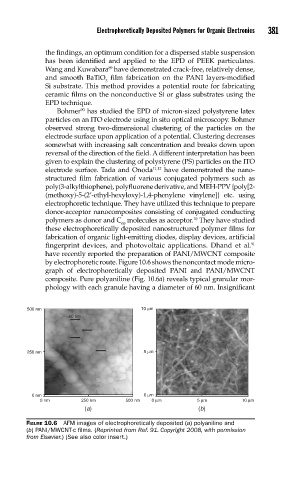
have recently reported the preparation of PANI/MWCNT composite
by electrophoretic route. Figure 10.6 shows the noncontact mode micro-
graph of electrophoretically deposited PANI and PANI/MWCNT
composite. Pure polyaniline (Fig. 10.6a) reveals typical granular mor-
phology with each granule having a diameter of 60 nm. Insignificant
500 nm 10 μm
60 nm
250 nm 5 μm
0 nm 0 μm
0 nm 250 nm 500 nm 0 μm 5 μm 10 μm
(a) (b)
FIGURE 10.6 AFM images of electrophoretically deposited (a) polyaniline and
(b) PANI/MWCNT-c fi lms. (Reprinted from Ref. 91. Copyright 2008, with permission
from Elsevier.) (See also color insert.)