
Page 406 - Organic Electronics in Sensors and Biotechnology
P. 406
Electrophoretically Deposited Polymers for Organic Electronics 383
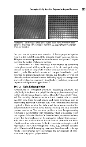
FIGURE 10.7 SEM images of colloidal crystal made from 300 nm PS latex
spheres. (Reprinted with permission from Ref. 93. Copyright 2008, American
Chemical Society.)
the spectrum of spontaneous emission of the impregnated species
results in the redistribution of the emission energy in such a system.
This phenomenon represents both fundamental and practical impor-
tance for the design of photonic devices.
95
Dziomkina et al. have introduced a new method by combining
electrophoresis and a lithographic approach for electrode patterning
that can be used for the growth of either colloidal monolayers or col-
loidal crystals. The method controls and changes the colloidal crystal
structure by introducing different patterns in a dielectric layer on top
of the electrodes used as substrates. Achieving highly accurate growth
and control of packing symmetry in colloidal crystals is of paramount
importance for photonic applications. 96
10.3.2 Light-Emitting Diodes
Applications of conjugated polymers possessing solubility like
poly(3-alkylthiophene) and poly(2,5-dialkoxy-p-phenylene vinylene)
to thin-film electronic devices, such as LEDs, have been widely stud-
ied. The solubility of these materials makes it possible to be processed
into thin solid films through simple and cheap techniques such as
spin coating. However, when thin films with submicron thickness are
required, a dilute solution has to be used. In such cases, most of the
polymer solution is blown away during spinning, and only a limited
portion remains as film. Another problem is that the spin-coating
technique is incompatible with patterning, which is necessary when
one targets a full-color display. On the other hand, recent studies have
shown that the morphology of the conjugated polymer film consider-
ably affects the performance of devices such as photocells and field-
effect transistors. In the case of field-effect transistors using spin-coated
regioregular poly(3-hexylthiophene) films, e.g., different solvents
yield different mobilities ranging over more than three orders of mag-
nitude. These findings have encouraged the development of nano-
structured conjugated polymer films.