
Page 226 - Phase-Locked Loops Design, Simulation, and Applications
P. 226
MIXED-SIGNAL PLL APPLICATIONS PART 1: INTEGER-N FREQUENCY
SYNTHESIZERS Ronald E. Best 137
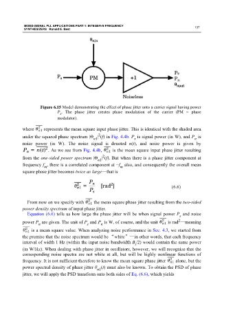
Figure 6.15 Model demonstrating the effect of phase jitter onto a carrier signal having power
P . The phase jitter creates phase modulation of the carrier (PM = phase
s
modulator).
where represents the mean square input phase jitter. This is identical with the shaded area
2
under the squared phase spectrum |Θ | (f) in Fig. 4.4b. P is signal power (in W), and P is
n1 s n
noise power (in W). The noise signal is denoted n(t), and noise power is given by
. As we see from Fig. 4.4b, is the mean square input phase jitter resulting
2
from the one-sided power spectrum |Θ | (f). But when there is a phase jitter component at
n1
frequency f , there is a correlated component at −f also, and consequently the overall mean
m m
square phase jitter becomes twice as large—that is
(6.6)
From now on we specify with the mean square phase jitter resulting from the two-sided
power density spectrum of input phase jitter.
Equation (6.6) tells us how large the phase jitter will be when signal power P and noise
s
2
power P are given. The unit of P and P is W, of course, and the unit is rad —meaning
n s n
is a mean square value. When analyzing noise performance in Sec. 4.3, we started from
the premise that the noise spectrum would be “white”—in other words, that each frequency
interval of width 1 Hz (within the input noise bandwidth B /2) would contain the same power
i
(in W/Hz). When dealing with phase jitter in oscillators, however, we will recognize that the
corresponding noise spectra are not white at all, but will be highly nonlinear functions of
frequency. It is not sufficient therefore to know the mean square phase jitter alone, but the
power spectral density of phase jitter θ (t) must also be known. To obtain the PSD of phase
n1
jitter, we will apply the PSD transform onto both sides of Eq. (6.6), which yields