
Page 92 - Photonics Essentials an introduction with experiments
P. 92
Photoconductivity
86 Photonic Devices
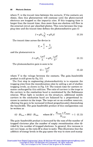
where T r is the transit time between the contacts. If the contacts are
ohmic, then this photocurrent will continue until the photo-excited
electrons are trapped on the impurity sites. If this trapping time is
longer than the transit time, then more than one electron will flow in
the external circuit per absorbed photon. This ratio between the trap-
ping time and the transit time defines the photoconductive gain G:
e
I = qN = qN G (5.10)
T r
The transit time across the device is
L L
T r = =
v
and the photocurrent is
e e V
I = qN = qN (5.11)
L L 2
The photoconductive gain is seen to be
e V
G = (5.12)
L 2
where V is the voltage between the contacts. The gain–bandwidth
product is still given by Eq. 5.5.
The first step in engineering photoconductivity is to separate the
trapping sites from the recombination sites by adding a set of shallow
trapping levels, as shown in Fig. 5.9. The transit time for carriers re-
mains unchanged by this addition. The ratio of carriers in the traps to
the carriers in the conduction band is maintained by the Boltzmann
relation. When light is incident on the structure, additional mobile
carriers in the conduction band are balanced by a proportional in-
crease in carriers in the traps. The traps act as an overflow reservoir,
allowing the gain to be increased without proportionately diminishing
the bandwidth. The gain bandwidth product of this configuration can
be written as
N traps + P empty
(G·B) new = M(G·B) old , where M = 1 (5.13)
N traps
The gain–bandwidth product is increased by the sum of the number of
trapped electrons plus the number of empty recombination sites di-
vided by the number of trapped electrons. In general, this increase is
not very large, so the ratio M is close to unity. This illustrates that the
addition of energy levels in the gap opens the way to store and manip-
Downloaded from Digital Engineering Library @ McGraw-Hill (www.digitalengineeringlibrary.com)
Copyright © 2004 The McGraw-Hill Companies. All rights reserved.
Any use is subject to the Terms of Use as given at the website.