
Page 184 - Power Electronic Control in Electrical Systems
P. 184
//SYS21/F:/PEC/REVISES_10-11-01/075065126-CH005.3D ± 172 ± [153±176/24] 17.11.2001 10:15AM
172 Power semiconductor devices and converter hardware issues
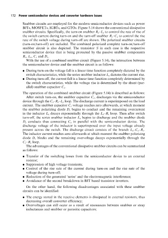
Snubber circuits are employed for the modern semiconductor devices such as power
BJTs, MOSFETs, IGBTs, and GTOs. Figure 5.14 shows the conventional dissipative
snubber circuits. Specifically, the turn-on snubber R s ±L s to control the rate of rise of
the switch current during turn-on and the turn-off snubber R s ±C s to control the rise
rate of the switch voltage during turn-off are shown. The polarized snubber circuits
(turn-on/turn-off) are included. The combined polarized complete turn-on/turn-off
snubber circuit is also depicted. The transistor S in each case is the respective
semiconductor device that is being protected by the passive snubber components
R s , L s , C s and D s .
With the use of a combined snubber circuit (Figure 5.14), the interaction between
the semiconductor device and the snubber circuit is as follows:
. During turn-on the voltage fall is a linear time function completely dictated by the
switch characteristics, while the series snubber inductor L s dictates the current rise.
. During turn-off, the current fall is a linear time function completely determined by
the switch characteristics, while the voltage rise is determined by the shunt (par-
allel) snubber capacitor C s .
The operation of the combined snubber circuit (Figure 5.14) is described as follows:
After switch turn-on, the snubber capacitor C s , discharges via the semiconductor
device through the C s ±R s ±L s loop. The discharge current is superimposed on the load
current. The snubber capacitor C s voltage reaches zero afterwards, at which moment
the snubber polarizing diode D s begins to conduct and the remaining overcurrent
in the inductor L s decays exponentially through the L s ±R s loop. Then after switch
turn-off, the series snubber inductor L s begins to discharge and the snubber diode
D s conducts thus connecting C s in parallel with the semiconductor device. The
discharge voltage of the inductor is superimposed over the input voltage already
present across the switch. The discharge circuit consists of the branch L s ±C s ±R s .
The inductor current reaches zero afterwards at which moment the snubber polarizing
diode D s blocks and the remaining overvoltage decays exponentially through the
C s ±R s loop.
The advantages of the conventional dissipative snubber circuits can be summarized
as follows:
. Transfer of the switching losses from the semiconductor device to an external
resistor;
. Suppression of high voltage transients;
. Control of the rise rate of the current during turn-on and the rise rate of the
voltage during turn-off;
. Reduction of the generated `noise' and the electromagnetic interference;
. Avoidance of the second breakdown in BJT based transistor inverters.
On the other hand, the following disadvantages associated with these snubber
circuits can be identified:
. The energy stored in the reactive elements is dissipated in external resistors, thus
decreasing overall converter efficiency;
. Overvoltages can still occur as a result of resonances between snubber or stray
inductances and snubber or parasitic capacitors;