
Page 185 - Power Electronic Control in Electrical Systems
P. 185
//SYS21/F:/PEC/REVISES_10-11-01/075065126-CH005.3D ± 173 ± [153±176/24] 17.11.2001 10:15AM
Power electronic control in electrical systems 173
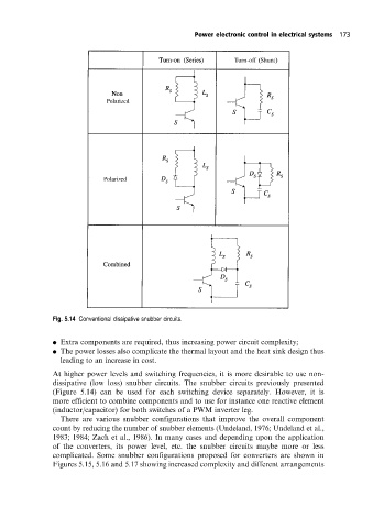
Fig. 5.14 Conventional dissipative snubber circuits.
. Extra components are required, thus increasing power circuit complexity;
. The power losses also complicate the thermal layout and the heat sink design thus
leading to an increase in cost.
At higher power levels and switching frequencies, it is more desirable to use non-
dissipative (low loss) snubber circuits. The snubber circuits previously presented
(Figure 5.14) can be used for each switching device separately. However, it is
more efficient to combine components and to use for instance one reactive element
(inductor/capacitor) for both switches of a PWM inverter leg.
There are various snubber configurations that improve the overall component
count by reducing the number of snubber elements (Undeland, 1976; Undeland et al.,
1983; 1984; Zach et al., 1986). In many cases and depending upon the application
of the converters, its power level, etc. the snubber circuits maybe more or less
complicated. Some snubber configurations proposed for converters are shown in
Figures 5.15, 5.16 and 5.17 showing increased complexity and different arrangements