
Page 376 - Power Electronic Control in Electrical Systems
P. 376
//SYS21/F:/PEC/REVISES_10-11-01/075065126-CH008.3D ± 357 ± [290±372/83] 17.11.2001 10:29AM
Power electronic control in electrical systems 357
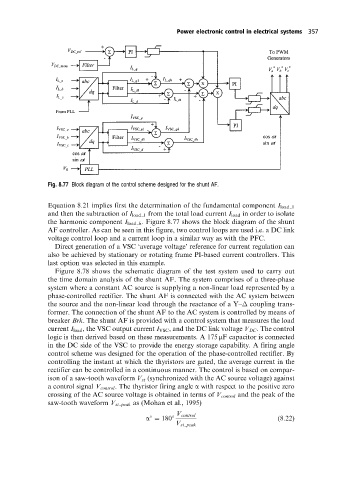
Fig. 8.77 Block diagram ofthe control scheme designed for the shunt AF.
Equation 8.21 implies first the determination of the fundamental component I load 1
and then the subtraction of I load 1 from the total load current I load in order to isolate
the harmonic component I load h . Figure 8.77 shows the block diagram of the shunt
AF controller. As can be seen in this figure, two control loops are used i.e. a DC link
voltage control loop and a current loop in a similar way as with the PFC.
Direct generation of a VSC `average voltage' reference for current regulation can
also be achieved by stationary or rotating frame PI-based current controllers. This
last option was selected in this example.
Figure 8.78 shows the schematic diagram of the test system used to carry out
the time domain analysis of the shunt AF. The system comprises of a three-phase
system where a constant AC source is supplying a non-linear load represented by a
phase-controlled rectifier. The shunt AF is connected with the AC system between
the source and the non-linear load through the reactance of a Y± coupling trans-
former. The connection of the shunt AF to the AC system is controlled by means of
breaker Brk. The shunt AF is provided with a control system that measures the load
current I load , the VSC output current I VSC , and the DC link voltage V DC . The control
logic is then derived based on these measurements. A 175 mF capacitor is connected
in the DC side of the VSC to provide the energy storage capability. A firing angle
control scheme was designed for the operation of the phase-controlled rectifier. By
controlling the instant at which the thyristors are gated, the average current in the
rectifier can be controlled in a continuous manner. The control is based on compar-
ison of a saw-tooth waveform V st (synchronized with the AC source voltage) against
a control signal V control . The thyristor firing angle a with respect to the positive zero
crossing of the AC source voltage is obtained in terms of V control and the peak of the
saw-tooth waveform V st peak as (Mohan et al., 1995)
V control
a 180 (8:22)
V st peak